


I’m going to write a few posts about computer internals with the goal of explaining how modern kernels work. I hope to make them useful to enthusiasts and programmers who are interested in this stuff but don’t have experience with it. The focus is on Linux, Windows, and Intel processors. Internals are a hobby for me, I have written a fair bit of kernel-mode code but haven’t done so in a while. This first post describes the layout of modern Intel-based motherboards, how the CPU accesses memory and the system memory map.
我打算写一些涉及计算机内部原理的文章,用来向读者解释现代操作系统内核的工作原理。 希望能对在这方面没有经验,却又感兴趣的程序员和爱好者提供一些帮助。 文章主要关注的平台是Linux,Windows操作系统以及Intel系列的CPU。 我个人对计算机内部原理非常有兴趣,并且曾经写过一些内核模块代码,不过已经很久没写了。 开篇我们关注的是现代Intel主板的布局,CPU如何访问内存以及系统的内存映射。
To start off let’s take a look at how an Intel computer is wired up nowadays. The diagram below shows the main components in a motherboard and dubious color taste:
首先我们来看下现如今Intel计算机的内部布局。下图展现的就是主板的大部分组件。
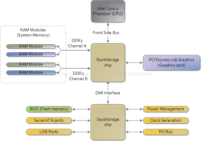
(补充: 北桥芯片用于与CPU、内存和AGP视频接口,这些接口具有很高的传输速率。北桥芯片还起着存储器控制作用,因此Intel把该芯片标号为MCH(Memory Controller Hub)芯片。南桥芯片用来管理低、中速的组件,例如,PCI总线、IDE硬盘接口、USB端口等,因此南桥芯片的名称为ICH(I/O Controller Hub))Diagram for modern motherboard. The northbridge and southbridge make up the chipset.
As you look at this, the crucial thing to keep in mind is that the CPU doesn’t really know anything about what it’s connected to. It talks to the outside world through its pins but it doesn’t care what that outside world is. It might be a motherboard in a computer but it could be a toaster, network router, brain implant, or CPU test bench. There are three main ways by which the CPU and the outside communicate: memory address space, I/O address space, and interrupts. We only worry about motherboards and memory for now.
正如你所看到的,其实CPU是完全不知道自己与哪些外部器件相连接的。 CPU仅仅通过自己的引脚与外界沟通,而它并不关心自己是与什么设备在沟通。 或许是另一台计算机的主板,或许是烤面包机,网络路由器,脑植入医疗设备,又或许是CPU测试仪。 CPU主要通过三种方式与外界通信:内存地址空间,IO地址空间,和中断。 我们目前只关注主板和内存。
In a motherboard the CPU’s gateway to the world is the front-side bus connecting it to the northbridge. Whenever the CPU needs to read or write memory it does so via this bus. It uses some pins to transmit the physical memory address it wants to write or read, while other pins send the value to be written or receive the value being read. An Intel Core 2 QX6600 has 33 pins to transmit the physical memory address (so there are 233 choices of memory locations) and 64 pins to send or receive data (so data is transmitted in a 64-bit data path, or 8-byte chunks). This allows the CPU to physically address 64 gigabytes of memory (233 locations * 8 bytes) although most chipsets only handle up to 8 gigs of RAM.
CPU通过前端总线与北桥芯片连接,作为与外界通信的桥梁。 无论何时,CPU都可以通过前端总线来读写内存。 CPU通过一些引脚来传送想要读写物理内存的地址,同时通过另一些引脚来发送将要写入内存的数据或者接收从内存读取到的数据。 Intel Core 2 QX6600 用33个引脚来传送物理内存地址(因此共有233 个内存地址),并且用64个引脚来发送或接收数据(所以数据在64位通道中传输,也就是8字节的数据块)。 因此CPU可以访问64G的物理内存(233*8字节),尽管多数芯片组只能处理8G大小的物理内存。
Now comes the rub. We’re used to thinking of memory only in terms of RAM, the stuff programs read from and write to all the time. And indeed most of the memory requests from the processor are routed to RAM modules by the northbridge. But not all of them. Physical memory addresses are also used for communication with assorted devices on the motherboard (this communication is calledmemory-mapped I/O). These devices include video cards, most PCI cards (say, a scanner or SCSI card), and also the flash memory that stores the BIOS.
那么现在的问题是,通常一提起内存我们仅仅联想到RAM,以为程序一直读写的就只是RAM。 的确,绝大多数来自CPU的内存访问请求都被北桥芯片映射到了RAM。 但是,注意,不是全部。 物理内存同样可以用来与主板上的各种设备通信(这种通信方式被称为I/O内存映射)。 这些设备包括显卡,大多数PCI卡(比如,扫描仪,或者是SCSI卡),也包括存储BIOS的flash存储器。
When the northbridge receives a physical memory request it decides where to route it: should it go to RAM? Video card maybe? This routing is decided via the memory address map. For each region of physical memory addresses, the memory map knows the device that owns that region. The bulk of the addresses are mapped to RAM, but when they aren’t the memory map tells the chipset which device should service requests for those addresses. This mapping of memory addresses away from RAM modules causes the classic hole in PC memory between 640KB and 1MB. A bigger hole arises when memory addresses are reserved for video cards and PCI devices. This is why 32-bit OSes haveproblems using 4 gigs of RAM. In Linux the file /proc/iomem neatly lists these address range mappings. The diagram below shows a typical memory map for the first 4 gigs of physical memory addresses in an Intel PC:
当北桥芯片接收到来自CPU的物理内存访问请求时,它将决定应该把该物理地址映射到哪里:是映射到RAM呢?还是显卡呢? 这个映射过程是通过内存地址映射完成的。 内存地址映射知道物理内存地址的每一块区域所对应的设备。 大多数的物理地址都被映射到了RAM,但当请求的物理地址不是映射到RAM时,内存地址映射就告诉芯片组应该由哪一个设备来负责响应处理该物理地址请求。 在PC机物理内存地址中,地址640K到1M的范围内很多区域并不是映射到RAM的,而是映射到各种各样的设备的。 尤其当为视频卡和PIC设备预留物理内存地址时,该内存区域映射到RAM的地址空间就越小。 这也就是为什么32位的操作系统不能完全使用4G RAM内存的原因。在linux操作系统中,文件/process/iomem清晰地列出了这些地址范围的映射关系。 下图展现的是IntelPC机的前4G物理内存地址的典型的内存映射:
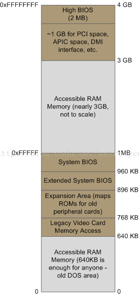
Memory layout for the first 4 gigabytes in an Intel system.
Actual addresses and ranges depend on the specific motherboard and devices present in the computer, but most Core 2 systems are pretty close to the above. All of the brown regions are mapped away from RAM. Remember that these are physical addresses that are used on the motherboard buses. Inside the CPU (for example, in the programs we run and write), the memory addresses are logical and they must be translated by the CPU into a physical address before memory is accessed on the bus.
实际的物理内存地址以及地址范围取决于计算机上不同的主板和设备,但是绝大多数Core 2系统的内存映射情况与上图很接近了。 图中所有棕色内存区域都不是映射到RAM中的。 请注意,这里提到的主板总线上的地址指的是物理内存地址。 在CPU内部(或者说,在我们运行与编写的程序里),内存地址指的是逻辑地址,在这些地址送上地址总线之前,CPU内部必须将这些逻辑地址转换成物理内存地址。
The rules for translation of logical addresses into physical addresses are complex and they depend on the mode in which the CPU is running (real mode, 32-bit protected mode, and 64-bit protected mode). Regardless of the translation mechanism, the CPU mode determines how much physical memory can be accessed. For example, if the CPU is running in 32-bit mode, then it is only capable of physically addressing 4 GB (well, there is an exception called physical address extension, but ignore it for now). Since the top 1 GB or so of physical addresses are mapped to motherboard devices the CPU can effectively use only ~3 GB of RAM (sometimes less – I have a Vista machine where only 2.4 GB are usable). If the CPU is in real mode, then it can only address 1 megabyte of physical RAM (this is the only mode early Intel processors were capable of). On the other hand, a CPU running in 64-bit mode can physically access 64GB (few chipsets support that much RAM though). In 64-bit mode it is possible to use physical addresses above the total RAM in the system to access the RAM regions that correspond to physical addresses stolen by motherboard devices. This is called reclaiming memory and it’s done with help from the chipset.
将逻辑地址转换成物理地址的过程是复杂的,并且依赖于CPU当前的运行模式(实模式,32位保护模式,和64位保护模式)。 我们要知道,不管CPU采用什么样的转换机制,CPU能够访问的物理内存地址范围大小是由CPU的运行模式决定的。 举例来说,如果CPU运行在32位保护模式下,那么它最大物理内存寻址范围是4G(当然,有个例外叫做物理内存扩展机制,目前先忽略这点)。 因为最上面的1G内存和那些被各种设备占用的物理内存,CPU真正能访问的大约只有3G的RAM(有时更少 -- 我的Vista机器上只有2.4G可用)。 如果CPU处于实模式下,那么它只能够访问到1M的物理内存(早期Intel CPU只有实模式这一种模式,1M是其最大的寻址范围)。此外,如果CPU运行在64位保护模式下,那么可以访问到64G的物理内存(目前很少有芯片组支持这么大的RAM)。 并且在64位模式下,CPU甚至可以访问超过RAM大小的物理内存地址,而这些地址通常是由主板上的其他设备使用的。 这叫做内存回收,当然这需要芯片组的支持才行。
That’s all the memory we need for the next post, which describes the boot process from power up until the boot loader is about to jump into the kernel. If you’d like to learn more about this stuff, I highly recommend the Intel manuals. I’m big into primary sources overall, but the Intel manuals in particular are well written and accurate. Here are some:
有了这些关于内存的认识,看下篇文章就很轻松了。 下篇文章中我们描述从计算机上电开始到bootloader即将跳转进内核的启动过程。 如果你希望更详细的了解这方面的内容,我强烈想您推荐Intel的手册。 我查询过很多资料,只有Intel的手册写的最详实和精准。 下面列出一些供参考:
- Datasheet for Intel G35 Chipset documents a representative chipset for Core 2 processors. This is the main source for this post.
- Datasheet for Intel Core 2 Quad-Core Q6000 Sequence is a processor datasheet. It documents each pin in the processor (there aren’t that many actually, and after you group them there’s really not a lot to it). Fascinating stuff, though some bits are arcane.
- The Intel Software Developer’s Manuals are outstanding. Far from arcane, they explain beautifully all sorts of things about the architecture. Volumes 1 and 3A have the good stuff (don’t be put off by the name, the “volumes” are small and you can read selectively).
- Pádraig Brady suggested that I link to Ulrich Drepper’s excellent paper on memory. It’s great stuff. I was waiting to link to it in a post about memory, but the more the merrier.


 125
125


 被折叠的 条评论
为什么被折叠?
被折叠的 条评论
为什么被折叠?
 到【灌水乐园】发言


