


1. SPI总线结构
SPI串行外设接口,是一种高速的,全双工,同步的通信总线。采用主从模式架构,支持多个slave,一般仅支持单Master
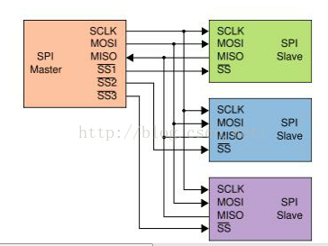
SPI接口共有4根信号线,分别是:
设备选择线(SS)、时钟线(SCK)、串行输出数据线(MOSI)、串行输入数据线(MISO).

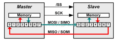
2. 数据传输过程
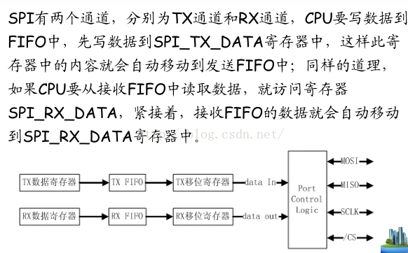
主节点通过MOSI线输出数据,从节点在SIMO处从主节点读取数据。同时,也通过SMOI输出MSB(最高位),
主节点会在MISO处读取从节点的数据,整个过程将一直持续,直至交换完所有的数据。
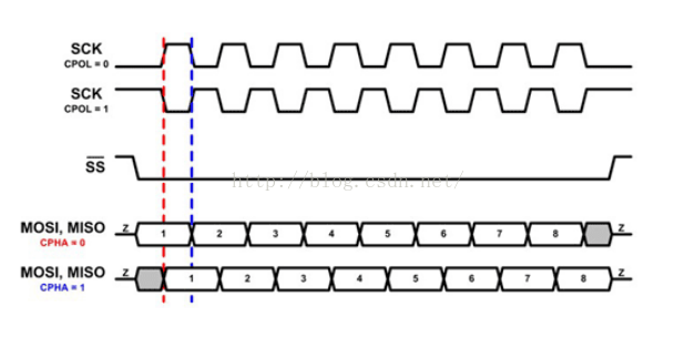
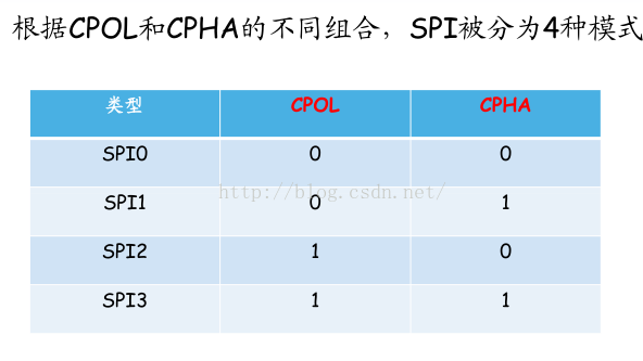
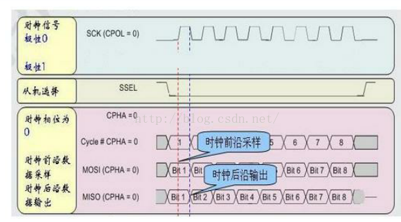
3. 总线时序

SPI裸机驱动程序设计:
1. SPI控制器工作流程
开发板上没有SPI外设,这里贴上别人整过SPI裸机驱动测试的链接:
http://blog.chinaunix.net/uid-24219701-id-3748675.html
http://blog.csdn.net/cp1300/article/details/8041760
http://blog.csdn.net/wanyeye/article/details/42494559
SPI子系统架构:
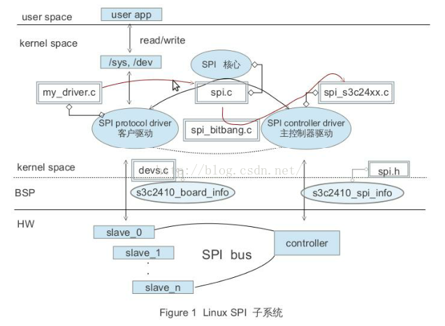
1. SPI核心
SPI控制器驱动和设备驱动之间的纽带,它提供了SPI控制器驱动和设备驱动的注册、注销方法等。
2. SPI控制器驱动
对SPI控制器驱动的实现
3. SPI设备驱动
对SPI从设备的驱动实现,如 spi flash
首先看看SPI核心驱动中的源码:
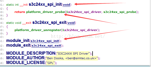
还是先上初始化模块部分:可以看到也是平台总线驱动模型!直接跳到probe函数中(本文件中的probe函数)
static int __init s3c24xx_spi_probe(struct platform_device *pdev)static int __init s3c24xx_spi_probe(struct platform_device *pdev)
{
struct s3c2410_spi_info *pdata;
struct s3c24xx_spi *hw;
struct spi_master *master;
struct resource *res;
int err = 0;
master = spi_alloc_master(&pdev->dev, sizeof(struct s3c24xx_spi));
if (master == NULL) {
dev_err(&pdev->dev, "No memory for spi_master\n");
err = -ENOMEM;
goto err_nomem;
}
hw = spi_master_get_devdata(master);
memset(hw, 0, sizeof(struct s3c24xx_spi));
hw->master = spi_master_get(master);
hw->pdata = pdata = pdev->dev.platform_data;
hw->dev = &pdev->dev;
if (pdata == NULL) {
dev_err(&pdev->dev, "No platform data supplied\n");
err = -ENOENT;
goto err_no_pdata;
}
platform_set_drvdata(pdev, hw);
init_completion(&hw->done);
/* initialise fiq handler */
s3c24xx_spi_initfiq(hw);
/* setup the master state. */
/* the spi->mode bits understood by this driver: */
master->mode_bits = SPI_CPOL | SPI_CPHA | SPI_CS_HIGH;
master->num_chipselect = hw->pdata->num_cs;
master->bus_num = pdata->bus_num;
/* setup the state for the bitbang driver */
hw->bitbang.master = hw->master;
hw->bitbang.setup_transfer = s3c24xx_spi_setupxfer;
hw->bitbang.chipselect = s3c24xx_spi_chipsel;
hw->bitbang.txrx_bufs = s3c24xx_spi_txrx;
hw->master->setup = s3c24xx_spi_setup;
hw->master->cleanup = s3c24xx_spi_cleanup;
dev_dbg(hw->dev, "bitbang at %p\n", &hw->bitbang);
/* find and map our resources */
res = platform_get_resource(pdev, IORESOURCE_MEM, 0);
if (res == NULL) {
dev_err(&pdev->dev, "Cannot get IORESOURCE_MEM\n");
err = -ENOENT;
goto err_no_iores;
}
hw->ioarea = request_mem_region(res->start, resource_size(res),
pdev->name);
if (hw->ioarea == NULL) {
dev_err(&pdev->dev, "Cannot reserve region\n");
err = -ENXIO;
goto err_no_iores;
}
hw->regs = ioremap(res->start, resource_size(res));
if (hw->regs == NULL) {
dev_err(&pdev->dev, "Cannot map IO\n");
err = -ENXIO;
goto err_no_iomap;
}
hw->irq = platform_get_irq(pdev, 0);
if (hw->irq < 0) {
dev_err(&pdev->dev, "No IRQ specified\n");
err = -ENOENT;
goto err_no_irq;
}
err = request_irq(hw->irq, s3c24xx_spi_irq, 0, pdev->name, hw);//中断相关部分
if (err) {
dev_err(&pdev->dev, "Cannot claim IRQ\n");
goto err_no_irq;
}
hw->clk = clk_get(&pdev->dev, "spi");
if (IS_ERR(hw->clk)) {
dev_err(&pdev->dev, "No clock for device\n");
err = PTR_ERR(hw->clk);
goto err_no_clk;
}
/* setup any gpio we can */
if (!pdata->set_cs) {
if (pdata->pin_cs < 0) {
dev_err(&pdev->dev, "No chipselect pin\n");
goto err_register;
}
err = gpio_request(pdata->pin_cs, dev_name(&pdev->dev));
if (err) {
dev_err(&pdev->dev, "Failed to get gpio for cs\n");
goto err_register;
}
hw->set_cs = s3c24xx_spi_gpiocs;
gpio_direction_output(pdata->pin_cs, 1);
} else
hw->set_cs = pdata->set_cs;
s3c24xx_spi_initialsetup(hw);//硬件相关部分的初始化
/* register our spi controller */ //向SPI核心注册驱动
err = spi_bitbang_start(&hw->bitbang);
if (err) {
dev_err(&pdev->dev, "Failed to register SPI master\n");
goto err_register;
}
return 0;
err_register:
if (hw->set_cs == s3c24xx_spi_gpiocs)
gpio_free(pdata->pin_cs);
clk_disable(hw->clk);
clk_put(hw->clk);
err_no_clk:
free_irq(hw->irq, hw);
err_no_irq:
iounmap(hw->regs);
err_no_iomap:
release_resource(hw->ioarea);
kfree(hw->ioarea);
err_no_iores:
err_no_pdata:
spi_master_put(hw->master);
err_nomem:
return err;
}
硬件初始化部分:(这个和裸机驱动里面的差不多)
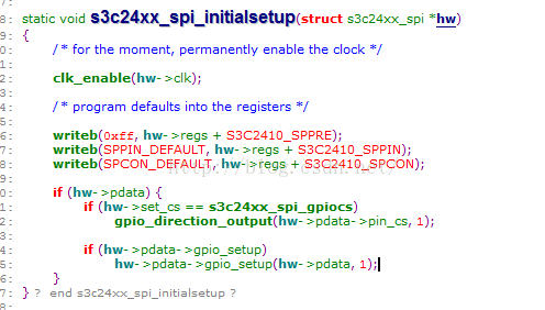
当然读写还有中断部分也是SPI的核心部分,看源码喽!
下面来简要介绍SPI从设备驱动程序设计:

内核源码文件m25p80.c 一种SPI接口的FLASH驱动!(SPI外设,这里先简单领略一下SPI外设驱动)
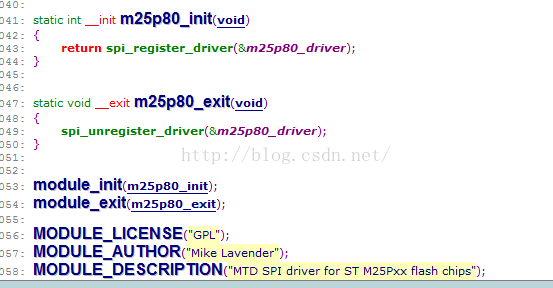
首先还是先看上面的模块初始化部分!这里先看看m25p80参数类型:
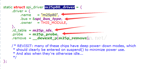
当驱动遇到了相应的设备的时候就会调用上面的m25p_probe函数
/*
 * board specific setup should have ensured the SPI clock used here
 * matches what the READ command supports, at least until this driver
 * understands FAST_READ (for clocks over 25 MHz).
 */
static int __devinit m25p_probe(struct spi_device *spi)
{
	const struct spi_device_id	*id = spi_get_device_id(spi);
	struct flash_platform_data	*data;
	struct m25p			*flash;
	struct flash_info		*info;
	unsigned			i;
	struct mtd_partition		*parts = NULL;
	int				nr_parts = 0;

	/* Platform data helps sort out which chip type we have, as
	 * well as how this board partitions it.  If we don't have
	 * a chip ID, try the JEDEC id commands; they'll work for most
	 * newer chips, even if we don't recognize the particular chip.
	 */
	data = spi->dev.platform_data;
	if (data && data->type) {
		const struct spi_device_id *plat_id;

		for (i = 0; i < ARRAY_SIZE(m25p_ids) - 1; i++) {
			plat_id = &m25p_ids[i];
			if (strcmp(data->type, plat_id->name))
				continue;
			break;
		}

		if (i < ARRAY_SIZE(m25p_ids) - 1)
			id = plat_id;
		else
			dev_warn(&spi->dev, "unrecognized id %s\n", data->type);
	}

	info = (void *)id->driver_data;

	if (info->jedec_id) {
		const struct spi_device_id *jid;

		jid = jedec_probe(spi);
		if (IS_ERR(jid)) {
			return PTR_ERR(jid);
		} else if (jid != id) {
			/*
			 * JEDEC knows better, so overwrite platform ID. We
			 * can't trust partitions any longer, but we'll let
			 * mtd apply them anyway, since some partitions may be
			 * marked read-only, and we don't want to lose that
			 * information, even if it's not 100% accurate.
			 */
			dev_warn(&spi->dev, "found %s, expected %s\n",
				 jid->name, id->name);
			id = jid;
			info = (void *)jid->driver_data;
		}
	}

	flash = kzalloc(sizeof *flash, GFP_KERNEL);
	if (!flash)
		return -ENOMEM;
	flash->command = kmalloc(MAX_CMD_SIZE + FAST_READ_DUMMY_BYTE, GFP_KERNEL);
	if (!flash->command) {
		kfree(flash);
		return -ENOMEM;
	}

	flash->spi = spi;
	mutex_init(&flash->lock);
	dev_set_drvdata(&spi->dev, flash);

	/*
	 * Atmel, SST and Intel/Numonyx serial flash tend to power
	 * up with the software protection bits set
	 */

	if (JEDEC_MFR(info->jedec_id) == CFI_MFR_ATMEL ||
	    JEDEC_MFR(info->jedec_id) == CFI_MFR_INTEL ||
	    JEDEC_MFR(info->jedec_id) == CFI_MFR_SST) {
		write_enable(flash);
		write_sr(flash, 0);
	}

	if (data && data->name)
		flash->mtd.name = data->name;
	else
		flash->mtd.name = dev_name(&spi->dev);

	flash->mtd.type = MTD_NORFLASH;
	flash->mtd.writesize = 1;
	flash->mtd.flags = MTD_CAP_NORFLASH;
	flash->mtd.size = info->sector_size * info->n_sectors;
	flash->mtd.erase = m25p80_erase;
	flash->mtd.read = m25p80_read;

	/* sst flash chips use AAI word program */
	if (JEDEC_MFR(info->jedec_id) == CFI_MFR_SST)
		flash->mtd.write = sst_write;
	else
		flash->mtd.write = m25p80_write;

	/* prefer "small sector" erase if possible */
	if (info->flags & SECT_4K) {
		flash->erase_opcode = OPCODE_BE_4K;
		flash->mtd.erasesize = 4096;
	} else {
		flash->erase_opcode = OPCODE_SE;
		flash->mtd.erasesize = info->sector_size;
	}

	if (info->flags & M25P_NO_ERASE)
		flash->mtd.flags |= MTD_NO_ERASE;

	flash->mtd.dev.parent = &spi->dev;
	flash->page_size = info->page_size;

	if (info->addr_width)
		flash->addr_width = info->addr_width;
	else {
		/* enable 4-byte addressing if the device exceeds 16MiB */
		if (flash->mtd.size > 0x1000000) {
			flash->addr_width = 4;
			set_4byte(flash, info->jedec_id, 1);
		} else
			flash->addr_width = 3;
	}

	dev_info(&spi->dev, "%s (%lld Kbytes)\n", id->name,
			(long long)flash->mtd.size >> 10);

	DEBUG(MTD_DEBUG_LEVEL2,
		"mtd .name = %s, .size = 0x%llx (%lldMiB) "
			".erasesize = 0x%.8x (%uKiB) .numeraseregions = %d\n",
		flash->mtd.name,
		(long long)flash->mtd.size, (long long)(flash->mtd.size >> 20),
		flash->mtd.erasesize, flash->mtd.erasesize / 1024,
		flash->mtd.numeraseregions);

	if (flash->mtd.numeraseregions)
		for (i = 0; i < flash->mtd.numeraseregions; i++)
			DEBUG(MTD_DEBUG_LEVEL2,
				"mtd.eraseregions[%d] = { .offset = 0x%llx, "
				".erasesize = 0x%.8x (%uKiB), "
				".numblocks = %d }\n",
				i, (long long)flash->mtd.eraseregions[i].offset,
				flash->mtd.eraseregions[i].erasesize,
				flash->mtd.eraseregions[i].erasesize / 1024,
				flash->mtd.eraseregions[i].numblocks);


	/* partitions should match sector boundaries; and it may be good to
	 * use readonly partitions for writeprotected sectors (BP2..BP0).
	 */
	if (mtd_has_cmdlinepart()) {
		static const char *part_probes[]
			= { "cmdlinepart", NULL, };

		nr_parts = parse_mtd_partitions(&flash->mtd,
						part_probes, &parts, 0);
	}

	if (nr_parts <= 0 && data && data->parts) {
		parts = data->parts;
		nr_parts = data->nr_parts;
	}

#ifdef CONFIG_MTD_OF_PARTS
	if (nr_parts <= 0 && spi->dev.of_node) {
		nr_parts = of_mtd_parse_partitions(&spi->dev,
						   spi->dev.of_node, &parts);
	}
#endif

	if (nr_parts > 0) {
		for (i = 0; i < nr_parts; i++) {
			DEBUG(MTD_DEBUG_LEVEL2, "partitions[%d] = "
			      "{.name = %s, .offset = 0x%llx, "
			      ".size = 0x%llx (%lldKiB) }\n",
			      i, parts[i].name,
			      (long long)parts[i].offset,
			      (long long)parts[i].size,
			      (long long)(parts[i].size >> 10));
		}
		flash->partitioned = 1;
	}

	return mtd_device_register(&flash->mtd, parts, nr_parts) == 1 ?
		-ENODEV : 0;  //注册一个mtd设备 硬盘分区 初始化部分一个很重要的操作
}
这里先重点关注一下write,就是驱动是如何把数据通过SPI总线写入FLASH中
/*
* Write an address range to the flash chip. Data must be written in
* FLASH_PAGESIZE chunks. The address range may be any size provided
* it is within the physical boundaries.
*/
static int m25p80_write(struct mtd_info *mtd, loff_t to, size_t len,
size_t *retlen, const u_char *buf)
{
struct m25p *flash = mtd_to_m25p(mtd);
u32 page_offset, page_size;
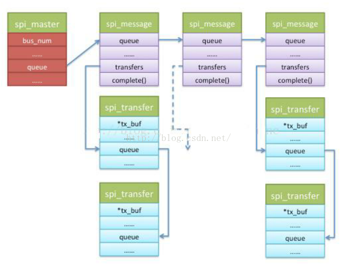
struct spi_transfer t[2];//这个结构和下面一行的结构非常重要 可以看看结合上面的图来看
struct spi_message m;
DEBUG(MTD_DEBUG_LEVEL2, "%s: %s %s 0x%08x, len %zd\n",
dev_name(&flash->spi->dev), __func__, "to",
(u32)to, len);
*retlen = 0;
/* sanity checks */
if (!len)
return(0);
if (to + len > flash->mtd.size)
return -EINVAL;
spi_message_init(&m);//初始化
memset(t, 0, (sizeof t));//数组清零
t[0].tx_buf = flash->command;//命令和数据分开 其实都是数据
t[0].len = m25p_cmdsz(flash);
spi_message_add_tail(&t[0], &m);//挂到message中 链表 准确的说是队列
t[1].tx_buf = buf;
spi_message_add_tail(&t[1], &m);//挂到message中
mutex_lock(&flash->lock);
/* Wait until finished previous write command. */
if (wait_till_ready(flash)) {
mutex_unlock(&flash->lock);
return 1;
}
write_enable(flash);
/* Set up the opcode in the write buffer. */
flash->command[0] = OPCODE_PP;
m25p_addr2cmd(flash, to, flash->command);
page_offset = to & (flash->page_size - 1);
/* do all the bytes fit onto one page? */
if (page_offset + len <= flash->page_size) {
t[1].len = len;
spi_sync(flash->spi, &m);//把message提交给控制器处理 控制器在合适的时候发送到SPI总线上去
*retlen = m.actual_length - m25p_cmdsz(flash);
} else {
u32 i;
/* the size of data remaining on the first page */
page_size = flash->page_size - page_offset;
t[1].len = page_size;
spi_sync(flash->spi, &m);
*retlen = m.actual_length - m25p_cmdsz(flash);
/* write everything in flash->page_size chunks */
for (i = page_size; i < len; i += page_size) {
page_size = len - i;
if (page_size > flash->page_size)
page_size = flash->page_size;
/* write the next page to flash */
m25p_addr2cmd(flash, to + i, flash->command);
t[1].tx_buf = buf + i;
t[1].len = page_size;
wait_till_ready(flash);
write_enable(flash);
spi_sync(flash->spi, &m);
*retlen += m.actual_length - m25p_cmdsz(flash);
}
}
mutex_unlock(&flash->lock);
return 0;
}上面的的其中一张函数调用关系图分析的比较详细!


 被折叠的 条评论
为什么被折叠?
被折叠的 条评论
为什么被折叠?
 到【灌水乐园】发言


