/*
 * Originates from Samsung's u-boot 1.1.6 port to S5PC1xx
 *
 * Copyright (C) 2009 Samsung Electrnoics
 * Inki Dae <inki.dae@samsung.com>
 * Heungjun Kim <riverful.kim@samsung.com>
 * Minkyu Kang <mk7.kang@samsung.com>
 * Kyungmin Park <kyungmin.park@samsung.com>
 *
 * See file CREDITS for list of people who contributed to this
 * project.
 *
 * This program is free software; you can redistribute it and/or
 * modify it under the terms of the GNU General Public License as
 * published by the Free Software Foundation; either version 2 of
 * the License, or (at your option) any later version.
 *
 * This program is distributed in the hope that it will be useful,
 * but WITHOUT ANY WARRANTY; without even the implied warranty of
 * MERCHANTABILITY or FITNESS FOR A PARTICULAR PURPOSE.  See the
 * GNU General Public License for more details.
 *
 * You should have received a copy of the GNU General Public License
 * along with this program; if not, write to the Free Software
 * Foundation, Inc., 59 Temple Place, Suite 330, Boston,
 * MA 02111-1307 USA
 */

#include <config.h>

	.globl mem_ctrl_asm_init
mem_ctrl_asm_init:
	ldr r0, =0xe6000000	/*APB_DMC_BASE*/

	ldr r1, =0xe0000000	/*PRO_ID_BASE*/
	ldr r2, [r1]		/*PRO_ID regiser*/
	bic r2, #0xfffffdff

/******************** DLL initialization **************************/
	@ldr r1, =0x6a101000
	ldr r1, =0x50101000
	str r1, [r0, #0x18]	/*PHY control 0 register*/

	@ldr r1, =0x000084f4
	ldr r1, =0x000000f6
	str r1, [r0, #0x1c]	/*PHY control 1 register*/

	ldr r1, =0x00000000
	str r1, [r0, #0x20]	/*PHY control 2 register*/

	@ldr r1, =0x6A101002				@DLL on
	ldr r1, =0x50101002
	str r1, [r0, #0x18]	/*PHY control 0 register*/

	@ldr r1, =0x6A101003				@Dll start
	ldr r1, =0x50101003
	str r1, [r0, #0x18]	/*PHY control 0 register*/

	ldr r1, =0x50101003
	str r1, [r0, #0x18]	/*PHY control 0 register*/

	ldr r1, =0x50101001
	str r1, [r0, #0x18]	/*PHY control 0 register*/

/************************** DLL initialization - END ************************/

	@ldr     r1, =0x0FF01010			@auto refresh off
	ldr 	r1, =0xFF001010
	str     r1, [r0, #0x0]	/*e6000000 = controller control register*/

	@ldr     r1, =0x00212400			@ BL=4 , 2 chip , DDR2
	ldr r1, =0xff202400
	str     r1, [r0, #0x4]	/*e6000004 = memory control register*/

	@ 128MB config , 8banks , linear, Row=13bit,COL=10bit
	@ldr	r1, =0x20F01313
	ldr r1, =0x20e00313
	str	r1, [r0, #0x8]

	@ldr	r1, =0x40F01313
	ldr r1, =0x30e00323
	str	r1, [r0, #0xc]

	ldr     r1, =0x20000000
	str     r1, [r0, #0x14]	/*precharge policy configuration register*/

	@ldr     r1, =0x00100004
	@str     r1, [r0, #0x28]	/*precharge policy configuration register*/


	/******************************************************************/

	@ldr	r1, =0x0000050e
	ldr r1, =0x00000400
	str     r1, [r0, #0x30]	/*AC timing register for auto refresh of memory*/

	@ldr	r1, =0x16233297			@TimingRow 	 @166MHz
	ldr r1, =0x16233287
	str     r1, [r0, #0x34]	/*AC timing register for the row of memory*/

@;	ldr	r1, =0x24250304			@CL=5
	@ldr	r1, =0x23230000			@CL=3
	ldr r1, =0x23240304
	str	r1, [r0, #0x38]	/*AC timing register for the data of memory*/

	@ldr     r1, =0x07c80232                 @Timing Power
	ldr r1, =0x09c80232
	str     r1, [r0, #0x3c]	/*AC timing register for the power mode of memory*/

/************************ direct command for DDR2 ***********************/

	ldr     r1, =0x07000000                 @chip0 Deselect
	str     r1, [r0, #0x10]	/*memory direct command register*/

	ldr     r1, =0x01000000                 @chip0 PALL
	str     r1, [r0, #0x10]

	ldr     r1, =0x00020000                 @chip0 EMRS2
	str     r1, [r0, #0x10]

	ldr     r1, =0x00030000                 @chip0 EMRS3
	str     r1, [r0, #0x10]

	ldr     r1, =0x00010400	@chip0 EMRS1 (MEM DLL on = DQS# disable)
	str     r1, [r0, #0x10]

@;	ldr     r1, =0x00000552	@chip0 MRS (MEM DLL reset) CL=5, Burst Length=4
	ldr     r1, =0x00000542	@chip0 MRS (MEM DLL reset) CL=3, Burst Length=4
	str     r1, [r0, #0x10]

	ldr     r1, =0x01000000                  @chip0 PALL
	str     r1, [r0, #0x10]

	ldr     r1, =0x05000000                  @chip0 REFA
	str     r1, [r0, #0x10]

	ldr     r1, =0x05000000                  @chip0 REFA
	str     r1, [r0, #0x10]

@;	ldr     r1, =0x00000452 @chip0 MRS (MEM DLL unreset) , BL=4 , CL=5
	ldr     r1, =0x00000442 @chip0 MRS (MEM DLL unreset) , BL=4 , CL=3
	str     r1, [r0, #0x10]

	ldr     r1, =0x00010780                  @chip0 EMRS1 (OCD default)
	str     r1, [r0, #0x10]

	ldr     r1, =0x00010400 @chip0 EMRS1 (OCD exit)  Reduced Strength
	str     r1, [r0, #0x10]

/************************ direct command for DDR2 - END*******************/

	@ldr     r1, =0x00FF20B0			@ConControl auto refresh on
	ldr 	r1, =0xff01030
	str     r1, [r0, #0x0]	/*e6000000 = controller control register*/

	ldr 	r1, =0x00100004
	str		r1, [r0, #0x28]

	@ldr     r1, =0x00212413		        @ MemControl
	ldr		r1, =0x00202400
	str     r1, [r0, #0x4]	/*e6000000 = controller control register*/

	b	exit_cpu_init

exit_cpu_init:
	mov pc, lr
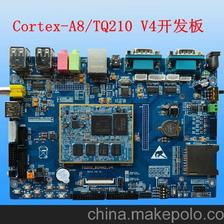
TQ210 —— s5pv210 mem_setup.S分析
最新推荐文章于 2018-08-01 15:33:54 发布


 1586
1586


 被折叠的 条评论
为什么被折叠?


