


One-atom-thin ‘silicene’ silicon transistors invented
原子大小数量级的硅烯晶体管宣告诞生
February 5, 2015

The first transistors made of silicene, the world’s thinnest silicon material, have been developed by researchers at The University of Texas at Austin’s Cockrell School of Engineering. The new material may allow for building dramatically faster, smaller, energy-efficient computer chips.
德克萨斯大学奥斯汀分校科克雷尔工程学院开发出了世界上第一款运用世界上最薄的硅材料--硅烯制造的晶体管。这种新型材料有望给人类带来引人注目的更快,更小,更高效的计算机芯片
Made of a one-atom-thick layer of silicon atoms, silicene has outstanding electrical properties but has until now proved difficult to produce and work with.
通过一个硅原子厚度生成的硅烯拥有过着无与伦比的电气特性,但却时至如今一直被证明是最难制造和驯服的。
Deji Akinwande, an assistant professor in the Cockrell School’s Department of Electrical and Computer Engineering, and his team, including lead researcher Li Tao, solved one of the major challenges surrounding silicene by demonstrating that it can be made into transistors.
科克雷尔工程学院助理教授Deji Akinwande以及他的团队,包括其首席研究员Li Tao,通过解决了围绕硅烯的一个主要问题来说明它是可以被用来生产晶体管的。Thinnest semiconductor material
最薄的半导体材料
These first-of-their-kind devices rely on the thinnest of any semiconductor material, a long-standing dream of the chip industry. Their work was published this week in the journal Nature Nanotechnology.
这些依赖最薄的半导体材料的同类首创设备 (天地会珠海分舵注:指的应该就是上面说的硅烯制造的晶体管)一直都是芯片届长期存在的梦想。Deji Akinwande以及他的团队的作品本周已经在《纳米技术》杂志中进行过报道。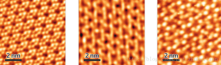
Until a few years ago, human-made silicene was a purely theoretical material. Looking at carbon-based graphene, another atom-thick material with promise for chip development, researchers speculated that silicon atoms could be structured in a broadly similar way.
直到几年前,非自然生成的硅烯还仅仅是一个纯理论存在的物质材料。通过比较另外一个给芯片研发带来希望的原子级别厚度的碳基材料 -- 石墨,研究人员猜测硅原子应该可以用一个相似的但更广阔的方式来进行组织起来而形成新的物质。
“Silicene, with its close chemical affinity to silicon, suggests an opportunity in the roadmap of the semiconductor industry,” Akinwande said. “The major breakthrough here is the efficient low-temperature manufacturing and fabrication of silicene devices for the first time.”
“硅烯,通过其与硅接近的化学特性,暗示着一个半导体产业蓝图的新机会,“Akinwande说道。”这里主要的突破就是首创性的高效的低发热量硅烯设备的生产工艺和装配工艺。“
Despite its promise for commercial adaptation, silicene has proved extremely difficult to create and work with because of its complexity and instability when exposed to air.
尽管其有望用于商业用途,但是硅烯已证明是非常难于生成和驯服的,皆因它是相当的复杂的,且一旦曝露于空气中将会变得极其的不稳定。
How to fabricate silicene
如何制造硅烯
To work around these issues, Akinwande teamed with Alessandro Molle at the Institute for Microelectronics and Microsystems in Agrate Brianza, Italy, to develop a new method for fabricating the silicene that reduces its exposure to air.
要去解决这些难题,Akinwande和在 Agrate Brianza的微电子和微系统研究所的Alessandro Molle团队联手开发了一个新的方法来在减少在空气曝光的情况下对硅烯进行制造。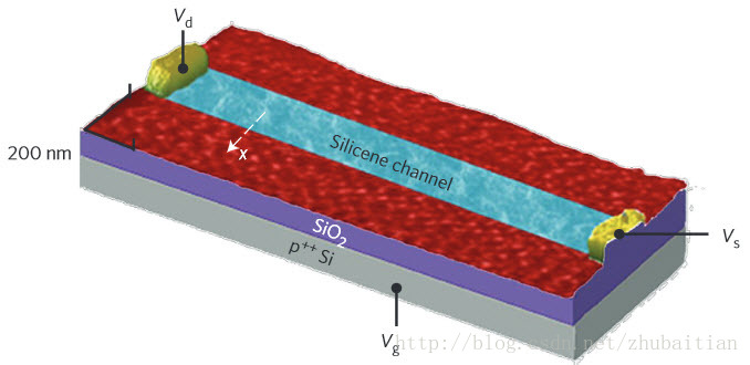
To start, the researchers let a hot vapor of silicon atoms condense onto a crystalline block of silver in a vacuum chamber. They then formed a silicene sheet on a thin layer of silver and added a nanometer-thick layer of alumina on top. Because of these protective layers, the team could safely peel it of its base and transfer it silver-side-up to an oxidized-silicon substrate. They were then able to gently scrape some of the silver to leave behind two islands of metal as electrodes, with a strip of silicene between them.
开始时,研究人员在真空室中运用高温气体的硅原子凝聚成一个银状晶体块。然后就会形成一个硅烯稀薄单层并覆盖上一个纳米层厚度的氧化铝在上面。因为有了这些保护层,团队就可以安全的刨去其表层并将该上层的银状晶体表面层转换成氧化硅。最后他们就可以小心的挂掉一部分银状晶体来留出两个独立的位置并在它们之间去掉硅烯的接触来作为电极使用了。
In the near-term, Akinwande will continue to investigate new structures and methods for creating silicene, which may lead to low-energy, high-speed digital computer chips.
近期内,Akinwande 会继续研究新的结构和方法来生产硅烯,以便给我们带来低功耗高速度的计算机芯片。
转载请尊重原创/译 | 微信公众号 | CSDN |
天地会珠海分舵 | 服务号:TechGoGoGo | http://blog.csdn.net/zhubaitian |
优秀资源推荐 | 地址 | 点评 |
DoctorQ博客 | http://testerhome.com/doctorq/topics
| 安卓自动化领域才俊,技术分享先 |


 1520
1520


 被折叠的 条评论
为什么被折叠?
被折叠的 条评论
为什么被折叠?
 到【灌水乐园】发言


