


SPI协议
Slave与Master
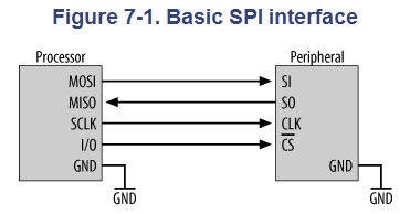
一般而言,提供clock的一方称为master。如下图(7-1)中的SCLK方向可知:Processor为master,而Peripheral为slave。
SPI设备接口
SPI uses four main signals:
- Master Out Slave In (MOSI)
- Master In Slave Out (MISO)
- Serial CLocK (SCLK or SCK) and Chip Select (CS) for the peripheral.
- Some processors have a dedicated chip select for SPI interfacing called Slave Select (SS).
SPI传输
SPI使用移位寄存器方式传输,示意图:

形成一个循环圈,任何时刻对于一个SPI设备而言都有移位输入和移位输出。
如果想只读或者只写,那么在读的时候需要发送一个dummy byte从而产生时钟;在写的时候简单的忽略读到的数据就可以了。
giga Nor flash:
All commands, addresses and data are shifted in and out of the device, beginning with the most significant bit on the
first rising edge of SCLK after CS# is driven low. Then, the one-byte command code must be shifted in to the device, most
significant bit first on SI, each bit being latched on the rising edges of SCLK.
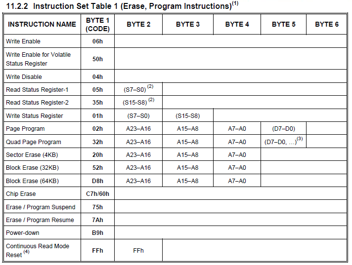
See Table2, every command sequence starts with a one-byte command code. Depending on the command, this
might be followed by address bytes, or by data bytes, or by both or none. CS# must be driven high after the last bit of the
command sequence has been shifted in. For the command of Read, Fast Read, Read Status Register or Release from
Deep Power-Down, and Read Device ID, the shifted-in command sequence is followed by a data-out sequence. CS# can
be driven high after any bit of the data-out sequence is being shifted out.
For the command of Page Program, Sector Erase, Block Erase, Chip Erase, Write Status Register, Write Enable,
Write Disable or Deep Power-Down command, CS# must be driven high exactly at a byte boundary, otherwise the
command is rejected, and is not executed. That is CS# must driven high when the number of clock pulses after CS# being
driven low is an exact multiple of eight. For Page Program, if at any time the input byte is not a full byte, nothing will happen
and WEL will not be reset.
1、SPI Flash (即SPI Nor Flash)是Nor Flash的一种;
2、NOR Flash根据数据传输的位数可以分为并行(Parallel)NOR Flash和串行(SPI)NOR Flash;
3、SPI Nor Flash每次传输一个bit位的数据,parallel Nor Flash每次传输多个bit位的数据(有x8和x16bit两种);
4、SPI Nor Flash比parallel便宜,接口简单点,但速度慢。
SPI传输的四种方式
根据时钟极性和时钟相位的不同共有四种,时钟极性和相位分别指:
- 时钟极性(CPOL-Clock Polarity):空闲时的极性高(
polarity high)或者低(polarity low)。 - 时钟相位(CPHA-CLock Phase):在上升沿还是下降沿采样数据。
四种模式用图说明如下:

将四种模式的采样时刻(Sampling edge)和数据变化时刻(Toggling edge)截取出来:

在逻辑分析仪上面的配置有可能稍有些不一样:
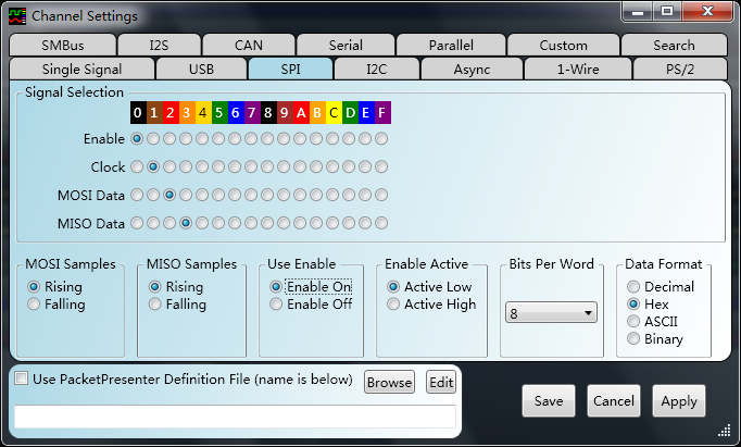
上图是一个虚拟逻辑分析仪软件上的SPI配置截图,除了通道选择和字长度配置外,它还有其他四个设置:
- MOSI Samples:如果是方式0和3,那么这里是上升沿,方式1和2应该配置为下降沿。看前面的方式说明图。
- MISO Samples:SO和SI在同一种方式下采样边缘一般是一样的,因此同上。
- Use Enable:是否使用CS Pin脚。
- Enable Active:这个是CS有效时候的电平。
示例:SPI寄存器配置
在某一个SoC上时钟极性和时钟相位的配置寄存器:
- 时钟极性配置(查看前面的4种模式图可以知道模式0和模式1应该是配置为0,另外两种配置为1):

- 时钟相位配置(查看前面的4种模式图可以知道模式1和模式3应该是配置为1【第二个edge】,另外两种配置为0):

- 一般除了方式设置外还需要对时钟速度配置,这个配置根据不同的SoC跟踪时钟如何分频过来就可以得出。并且需要注意不要超过Spi-Slave设备的最大速度。
SPI reset配置:
SPI Nor Flash
这里用EN25Q128为例,简略说明一下SPI的配置。这里使用模式0标准SPI模式(只用一根DO线)。
SPI-NorFlash的接线


 1万+
1万+

 被折叠的 条评论
为什么被折叠?
被折叠的 条评论
为什么被折叠?
 到【灌水乐园】发言


