


友晶公司的5 Mega Pixel Digital Camera Development Kit(或者1.3Mega Pixel Digital Camera Development Kit )中的VGA_Controller核,它以SDRAM为显存,通过双端口SDRAM控制器从SDRAM中取数据从而写入VGA接口(实际上中间还有一款DE2(DE2-70)上的DA转换芯片)在显示器上显示,而SDRAM控制器的另一端口则不断接收来自摄像头的图像数据往SDRAM中写入。它可以显示视频,但是却不可以由NiosII直接控制,实际上我们往往在NiosII处理器中做图像处理,比如视频解码。这就需要我们在双端口SDRAM控制器的写端口接到Nios II的avalon总线接口上。
接口部分所写的代码:
module sdramw (
// inputs:
avs_s1_address,
avs_s1_chipselect,
avs_s1_write,
avs_s1_writedata,
csi_clockreset_clk,
csi_clockreset_reset_n,
// outputs:
avs_s1_export_wr,
avs_s1_export_wrdata,
avs_s1_export_clk
);
output avs_s1_export_wr;
output [ 15: 0] avs_s1_export_wrdata;
output avs_s1_export_clk;
input avs_s1_address;
input avs_s1_chipselect;
input avs_s1_write;
input [ 31: 0] avs_s1_writedata;
input csi_clockreset_clk;
input csi_clockreset_reset_n;
wire avs_s1_export_wr;
wire avs_s1_export_clk;
wire [ 15: 0] avs_s1_export_wrdata;
sw_Controller the_sw_Controller
(
.avs_s1_address (avs_s1_address),
.avs_s1_chipselect (avs_s1_chipselect),
.avs_s1_export_wr (avs_s1_export_wr),
.avs_s1_export_wrdata (avs_s1_export_wrdata),
.avs_s1_export_clk (avs_s1_export_clk),
.avs_s1_write (avs_s1_write),
.avs_s1_writedata (avs_s1_writedata),
.csi_clockreset_clk (csi_clockreset_clk),
.csi_clockreset_reset_n (csi_clockreset_reset_n)
);
endmodule
/*
modified from
http://www.cnblogs.com/oomusou/archive/2008/10/24/de2_70_cmos_controller.html
Filename : CMOS_Controller.v
*/
module sw_Controller (
// Avalon clock interface siganals
input csi_clockreset_clk,
input csi_clockreset_reset_n,
// Signals for Avalon-MM slave port
input [1:0] avs_s1_address,
input avs_s1_chipselect,
input avs_s1_write,
input [31:0] avs_s1_writedata,
// Signals export to top module
output avs_s1_export_clk,
output reg avs_s1_export_wr,
output reg [15:0] avs_s1_export_wrdata
);
// Slave address constant
assign avs_s1_export_clk = csi_clockreset_clk;
// write to export
always@(posedge csi_clockreset_clk, negedge csi_clockreset_reset_n) begin
if (!csi_clockreset_reset_n) begin
avs_s1_export_wr <= 1'b0;
avs_s1_export_wrdata <= 16'hzzzz;
end
else begin
if (avs_s1_chipselect && avs_s1_write) begin
avs_s1_export_wr <= 1'b1;
avs_s1_export_wrdata <= avs_s1_writedata[15:0];
end
else begin
avs_s1_export_wr <= 1'b0;
avs_s1_export_wrdata <= 16'hzzzz;
end
end
end
endmodule
系统Top文件源码:
module DE2_70_D5M_XVGA (
//// Clock Input ////
input iTD1_CLK27,
output oTD1_RESET_N,
input iCLK_28, // 28.63636 MHz
input iCLK_50, // 50 MHz
input iCLK_50_2, // 50 MHz
input iCLK_50_3, // 50 MHz
input iCLK_50_4, // 50 MHz
input iEXT_CLOCK, // External Clock
//// Push Button ////
input [3:0] iKEY, // Pushbutton[3:0]
//// DPDT Switch ////
input [17:0] iSW, // Toggle Switch[17:0]
LED
output [8:0] oLEDG, // LED Green[8:0]
output [17:0] oLEDR, // LED Red[17:0]
/ SDRAM Interface ////
inout [31:0] DRAM_DQ, // SDRAM Data bus 32 Bits
output [12:0] oDRAM0_A, // SDRAM0 Address bus 12 Bits
output [12:0] oDRAM1_A, // SDRAM1 Address bus 12 Bits
output oDRAM0_LDQM0, // SDRAM0 Low-byte Data Mask
output oDRAM1_LDQM0, // SDRAM1 Low-byte Data Mask
output oDRAM0_UDQM1, // SDRAM0 High-byte Data Mask
output oDRAM1_UDQM1, // SDRAM1 High-byte Data Mask
output oDRAM0_WE_N, // SDRAM0 Write Enable
output oDRAM1_WE_N, // SDRAM1 Write Enable
output oDRAM0_CAS_N, // SDRAM0 Column Address Strobe
output oDRAM1_CAS_N, // SDRAM1 Column Address Strobe
output oDRAM0_RAS_N, // SDRAM0 Row Address Strobe
output oDRAM1_RAS_N, // SDRAM1 Row Address Strobe
output oDRAM0_CS_N, // SDRAM0 Chip Select
output oDRAM1_CS_N, // SDRAM1 Chip Select
output [1:0] oDRAM0_BA, // SDRAM0 Bank Address
output [1:0] oDRAM1_BA, // SDRAM1 Bank Address
output oDRAM0_CLK, // SDRAM0 Clock
output oDRAM1_CLK, // SDRAM0 Clock
output oDRAM0_CKE, // SDRAM0 Clock Enable
output oDRAM1_CKE, // SDRAM1 Clock Enable
//// Flash Interface ////
inout [14:0] FLASH_DQ, // FLASH Data bus 15 Bits (0 to 14)
inout FLASH_DQ15_AM1, // FLASH Data bus Bit 15 or Address A-1
output [25:0] oFLASH_A, // FLASH Address bus 26 Bits
output oFLASH_WE_N, // FLASH Write Enable
output oFLASH_RST_N, // FLASH Reset
output oFLASH_WP_N, // FLASH Write Protect /Programming Acceleration
input iFLASH_RY_N, // FLASH Ready/Busy output
output oFLASH_BYTE_N, // FLASH Byte/Word Mode Configuration
output oFLASH_OE_N, // FLASH Output Enable
output oFLASH_CE_N, // FLASH Chip Enable
//// SRAM Interface ////
inout [31:0] SRAM_DQ, // SRAM Data Bus 32 Bits
inout [3:0] SRAM_DPA, // SRAM Parity Data Bus
output [20:0] oSRAM_A, // SRAM Address bus 22 Bits
output oSRAM_ADSC_N, // SRAM Controller Address Status
output oSRAM_ADSP_N, // SRAM Processor Address Status
output oSRAM_ADV_N, // SRAM Burst Address Advance
output [3:0] oSRAM_BE_N, // SRAM Byte Write Enable
output oSRAM_CE1_N, // SRAM Chip Enable
output oSRAM_CE2, // SRAM Chip Enable
output oSRAM_CE3_N, // SRAM Chip Enable
output oSRAM_CLK, // SRAM Clock
output oSRAM_GW_N, // SRAM Global Write Enable
output oSRAM_OE_N, // SRAM Output Enable
output oSRAM_WE_N, // SRAM Write Enable
//// VGA ////
output oVGA_CLOCK, // VGA Clock
output oVGA_HS, // VGA H_SYNC
output oVGA_VS, // VGA V_SYNC
output oVGA_BLANK_N, // VGA BLANK
output oVGA_SYNC_N, // VGA SYNC
output [9:0] oVGA_R, // VGA Red[9:0]
output [9:0] oVGA_G, // VGA Green[9:0]
output [9:0] oVGA_B // VGA Blue[9:0]
);
//===========================================================================
// PARAMETER declarations
//===========================================================================
wire [12:0] oDRAM0_A_0; // SDRAM Address bus 12 Bits
wire oDRAM0_LDQM0_0; // SDRAM Low-byte Data Mask
wire oDRAM0_UDQM1_0; // SDRAM High-byte Data Mask
wire oDRAM0_WE_N_0; // SDRAM Write Enable
wire oDRAM0_CAS_N_0; // SDRAM Column Address Strobe
wire oDRAM0_RAS_N_0; // SDRAM Row Address Strobe
wire oDRAM0_CS_N_0; // SDRAM Chip Select
wire [1:0] oDRAM0_BA_0; // SDRAM Bank Address 0
wire oDRAM0_CLK_0; // SDRAM Clock
wire oDRAM0_CKE_0; // SDRAM Clock Enable
wire [12:0] oDRAM0_A_1; // SDRAM Address bus 12 Bits
wire oDRAM0_LDQM0_1; // SDRAM Low-byte Data Mask
wire oDRAM0_UDQM1_1; // SDRAM High-byte Data Mask
wire oDRAM0_WE_N_1; // SDRAM Write Enable
wire oDRAM0_CAS_N_1; // SDRAM Column Address Strobe
wire oDRAM0_RAS_N_1; // SDRAM Row Address Strobe
wire oDRAM0_CS_N_1; // SDRAM Chip Select
wire [1:0] oDRAM0_BA_1; // SDRAM Bank Address 0
wire oDRAM0_CLK_1; // SDRAM Clock
wire oDRAM0_CKE_1; // SDRAM Clock Enable
//wire CLK100;
reg pre_iKEY_3;
reg pre_iKEY_2;
wire [17:0] oLEDRm_0;
wire [7:0] oLEDGm_0,oLEDGm_1;
reg switch;
wire CPU_RESET_N;
wire CPU_CLK;
//========== FLASH
`define FLASH_WORD // use WORD mode of flash
`ifdef FLASH_WORD
wire FLASH_16BIT_IP_A0;
assign oFLASH_BYTE_N = 1'b1; // FLASH Byte/Word Mode Configuration
`else
assign oFLASH_BYTE_N = 1'b0; // FLASH Byte/Word Mode Configuration
`endif
assign oFLASH_RST_N = 1'b1; // FLASH Reset
assign oFLASH_WP_N = 1'b1; // FLASH Write Protect /Programming Acceleration
// iFLASH_RY_N, // FLASH Ready/Busy output
//========== SSRAM
assign oSRAM_ADSP_N = 1'b1; // SRAM Processor Address Status
assign oSRAM_ADV_N = 1'b1; // SRAM Burst Address Advance
assign oSRAM_CE2 = ~oSRAM_CE1_N;//1'b1; // SRAM Chip Enable
assign oSRAM_CE3_N = oSRAM_CE1_N;//1'b0; // SRAM Chip Enable
assign oSRAM_GW_N = 1'b1; // SRAM Global Write Enable
wire [1:0] SRAM_DUMMY_ADDR; // used to ignore the A0/A1 pin from Cypress SSRAM IP core
assign oSRAM_CLK = CPU_CLK;
//========== SDRAM
assign oDRAM1_CLK = CPU_CLK;
assign oTD1_RESET_N = 1'b1;
//======= NIOS CPU ======
wire [15:0] Read_DATA1;
wire [15:0] Read_DATA2;
wire VGA_CTRL_CLK;
wire Read;
wire sdram_ctrl_clk;
wire Nios_wr0;
wire Nios_clk0;
wire [15:0] Nios_wrdata0;
wire Nios_wr1;
wire Nios_clk1;
wire [15:0] Nios_wrdata1;
assign oTD1_RESET_N = 1'b1;
assign oVGA_CLOCK =~VGA_CTRL_CLK;
Reset_Delay delay1 (.iRST(iKEY[0]),.iCLK(iCLK_50),.oRESET(CPU_RESET_N));
PDF_SOPC u1 (
// 1) global signals:
.clk_50(iCLK_50_2),
.pll_c0_system(CPU_CLK),
.pll_c1_memory(oDRAM0_CLK_0),
//.pll_c2_audio(oAUD_XCK),//CLK_18M324),
.reset_n(CPU_RESET_N),
//.clk_25(iCLK_25),
// the_pio_button
.in_port_to_the_pio_button(iKEY),
// the_pio_green_led
.out_port_from_the_pio_green_led(oLEDGm_0),
// the_pio_red_led
.out_port_from_the_pio_red_led(oLEDRm_0),
// the_sdram (u2)
.zs_addr_from_the_sdram_u2(oDRAM1_A),
.zs_ba_from_the_sdram_u2(oDRAM1_BA),
.zs_cas_n_from_the_sdram_u2(oDRAM1_CAS_N),
.zs_cke_from_the_sdram_u2(oDRAM1_CKE),
.zs_cs_n_from_the_sdram_u2(oDRAM1_CS_N),
.zs_dq_to_and_from_the_sdram_u2(DRAM_DQ[31:16]),
.zs_dqm_from_the_sdram_u2({oDRAM1_UDQM1,oDRAM1_LDQM0}),
.zs_ras_n_from_the_sdram_u2(oDRAM1_RAS_N),
.zs_we_n_from_the_sdram_u2(oDRAM1_WE_N),
// the_tristate_bridge_avalon_slave (flash)
`ifdef FLASH_WORD
.address_to_the_cfi_flash({oFLASH_A[21:0],FLASH_16BIT_IP_A0}),
.data_to_and_from_the_cfi_flash({FLASH_DQ15_AM1,FLASH_DQ}),
`else
.address_to_the_cfi_flash({oFLASH_A[21:0],FLASH_DQ15_AM1}),
.data_to_and_from_the_cfi_flash(FLASH_DQ[7:0]),
`endif
.read_n_to_the_cfi_flash(oFLASH_OE_N),
.select_n_to_the_cfi_flash(oFLASH_CE_N),
.write_n_to_the_cfi_flash(oFLASH_WE_N),
// the_tristate_bridge_1_avalon_slave (ssram)
.address_to_the_ssram({oSRAM_A[17:0],SRAM_DUMMY_ADDR}),
.adsc_n_to_the_ssram(oSRAM_ADSC_N),
.bw_n_to_the_ssram(oSRAM_BE_N),
.bwe_n_to_the_ssram(oSRAM_WE_N),
.chipenable1_n_to_the_ssram(oSRAM_CE1_N),
.data_to_and_from_the_ssram((SRAM_DQ)),
.outputenable_n_to_the_ssram(oSRAM_OE_N),
// the_sdramw_inst0
.avs_s1_export_clk_from_the_sdramw_inst0(Nios_clk0),
.avs_s1_export_wr_from_the_sdramw_inst0(Nios_wr0),
.avs_s1_export_wrdata_from_the_sdramw_inst0(Nios_wrdata0),
// the_sdramw_inst1
.avs_s1_export_clk_from_the_sdramw_inst1(Nios_clk1),
.avs_s1_export_wr_from_the_sdramw_inst1(Nios_wr1),
.avs_s1_export_wrdata_from_the_sdramw_inst1(Nios_wrdata1)
);
vga_pll vga_pll0 (
.areset(!DLY_RST_0),
.inclk0(iCLK_50_3),
.c0(VGA_CTRL_CLK)
);
//assign VGA_CTRL_CLK = CCD_MCLK;
VGA_Controller vga0 (
// Host Side
.oRequest(Read),
.iRed({Read_DATA1[15:11],5'b11111}),
.iGreen({Read_DATA1[10:5],4'b1111}),
.iBlue({Read_DATA1[4:0],5'b11111}),
// VGA Side
.oVGA_R(oVGA_R),
.oVGA_G(oVGA_G),
.oVGA_B(oVGA_B),
.oVGA_H_SYNC(oVGA_HS),
.oVGA_V_SYNC(oVGA_VS),
.oVGA_SYNC(oVGA_SYNC_N),
.oVGA_BLANK(oVGA_BLANK_N),
// Control Signal
.iCLK(VGA_CTRL_CLK),
.iRST_N(DLY_RST_2),
.iZOOM_MODE_SW(iSW[16])
);
Reset_Delay_CCD reset0 (
.iCLK(iCLK_50),
.iRST(iKEY[0]),
.oRST_0(DLY_RST_0),
.oRST_1(DLY_RST_1),
.oRST_2(DLY_RST_2)
);
sdram_pll sdram_pll0 (
.inclk0(iCLK_50),
.c0(sdram_ctrl_clk),
.c1(oDRAM0_CLK)
//.c2(oDRAM1_CLK)
);
Sdram_Control_4Port sdram0 (
// HOST Side
.REF_CLK(iCLK_50),
.RESET_N(DLY_RST_0),
.CLK(sdram_ctrl_clk),
// FIFO Write Side 1
.WR1_DATA(Nios_wrdata0),
.WR1(Nios_wr0),
.WR1_ADDR(0),
.WR1_MAX_ADDR(1280*1024),
.WR1_LENGTH(9'h100),
.WR1_LOAD(1'b0),
.WR1_CLK(Nios_clk0),
// FIFO Write Side 2
.WR2_DATA(Nios_wrdata1),
.WR2(Nios_wr1),
.WR2_ADDR(24'h200000),
.WR2_MAX_ADDR(24'h200000+1280*1024),
.WR2_LENGTH(9'h100),
.WR2_LOAD(1'b0),
.WR2_CLK(Nios_clk1),
// FIFO Read Side 1
.RD1_DATA(Read_DATA1),
.RD1(Read),
.RD1_ADDR(0),
.RD1_MAX_ADDR(1280*1024),
.RD1_LENGTH(9'h100),
.RD1_LOAD(!DLY_RST_0),
.RD1_CLK(VGA_CTRL_CLK),
// FIFO Read Side 2
.RD2_DATA(Read_DATA2),
.RD2(Read),
.RD2_ADDR(24'h200000),
.RD2_MAX_ADDR(24'h200000+1280*1024),
.RD2_LENGTH(9'h100),
.RD2_LOAD(!DLY_RST_0),
.RD2_CLK(VGA_CTRL_CLK),
// SDRAM Side
.SA(oDRAM0_A[12:0]),
.BA(oDRAM0_BA),
.CS_N(oDRAM0_CS_N),
.CKE(oDRAM0_CKE),
.RAS_N(oDRAM0_RAS_N),
.CAS_N(oDRAM0_CAS_N),
.WE_N(oDRAM0_WE_N),
.DQ(DRAM_DQ[15:0]),
.DQM({oDRAM0_UDQM1_1,oDRAM0_LDQM0})
);
assign oLEDR = iSW ;
assign oLEDG = oLEDGm_0;
endmodule
C源码部分:
#include <stdio.h>
#include "io.h"
#include "system.h"
#include "rgb565_640x480.h"
//#include "data_grb_H.h"
int main()
{
unsigned int i;
for(i=0;i<1280*1024;i++){
if(i<640*480){
IOWR_16DIRECT(SDRAMW_INST0_BASE,0,rgb565[i]);
}
}
printf("Hello from Nios II!\n");
return 0;
}
显示效果图:
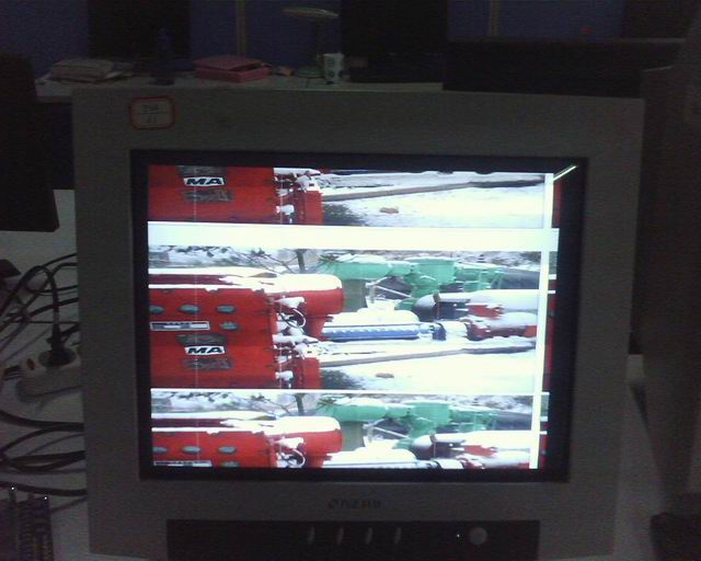
这种实现方案的一个弊端是,不好控制图像帧开始信号,图像容易在荧屏上飘移


 被折叠的 条评论
为什么被折叠?
被折叠的 条评论
为什么被折叠?
 到【灌水乐园】发言


