


vivado 的一个报错情况
ERROR: [Labtools 27-3412] Mismatch between the design programmed into the device ‘xc7a200t’ (JTAG device index = ‘0’
and the probes file(s) ‘\WIN2012-01\Development\elog\trial_images\elog_a7_top.ltx’.
The hw_probe ‘slot[0].if_inst/front_end_inst/dual_rgmii.rgmii_bridge_gen’ in the probes file has port index ‘4’. This port location for the ILA core at location (uuid_1CCDE7DB623B5320996586BD50DA0468), does not support a data probe.
.
Resolution:
- Ensure that the clock signal connected to the debug core and/or debug hub is clean and free-running.
- Ensure that the clock connected to the debug core and/or debug hub meets all timing constraints.
- Ensure that the JTAG clock frequency is 2.5x times slower than the frequency of the clock connected to your debug hub.
官方给的解决方案
将官方的解决方案
solution1
The clock net connected to dbg_hub is automatically selected by the tool based on the debug core configuration and connections.
However, you can change this clock net by modifying the “connect_debug_port” command in XDC.
The following are possible causes and solutions:
- The clock that is connected to dbg_hub is a non-free-running clock.
To check which clock net is connected to the dbg_hub, follow these steps in the Vivado GUI:
Open the Synthesized design or Implemented design -> Right click the dbg_hub core in the netlist hierarchy and select “Schematic” -> Double click the “clk” pin
If this clock is a non-free-running clock, change it to a free running one by modifying this command in XDC:
connect_debug_port dbg_hub/clk [get_nets <clock_net_name>]
修改连接在debug hub 的clk线,流程如下:
Open the Synthesized design or Implemented design -> Right click the dbg_hub core in the netlist hierarchy and select “Schematic” -> Double click the “clk” pin
If this clock is a non-free-running clock, change it to a free running one by modifying this command in XDC:
connect_debug_port dbg_hub/clk [get_nets <clock_net_name>]
solution 2
The clock is a free running clock but the signal integrity of this clock net is not good.
Check if the quality of this clock signal on the board is good or not. One example of this issue is if the daughter card connector is not inserted tightly (clock is coming from the daughter card).
翻译:
有这个clock 但是这个clock的质量太差了,监测一下板子上的clk的时钟信号如何
solution 3
Try the second solution mentioned in the warning message which is to use the other User Scan Chain number.
For example, the following are the steps to change to use Scan Chain number 2:
Change the C_USER_SCAN_CHAIN property of the dbg_hub core to 2. Please refer to (UG908) for how to change this property.
Manually launch hw_server in the Windows command prompt or a terminal on Linux:
hw_server -e "set xsdb-user-bscan <C_USER_SCAN_CHAIN 2>
翻译:
尽量还是使用solution 2 中提到的解决方案,但是如果还是有问题, 请采用将user scan charn 进行修改。
我遇到的报错以及我得解决过程
遇到的问题
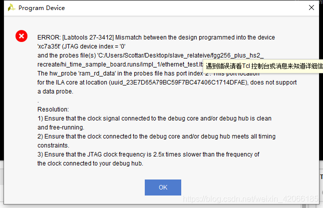
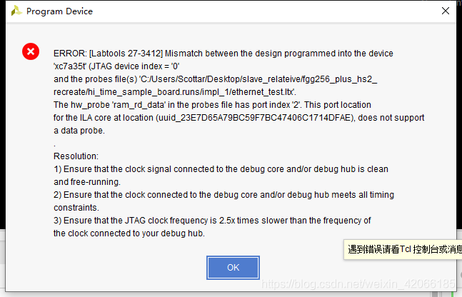
ERROR: [Labtools 27-3412] Mismatch between the design programmed into the device ‘xc7a35t’ (JTAG device index = ‘0’ and the probes file(s) ‘C:/Users/Scottar/Desktop/slave_relateive/fgg256_plus_hs2_ recreate/hi_time_sample_board.runs/impl_1/ethernet_test.ltx’. The hw_probe ‘ram_rd_data’ in the probes file has port index ‘2’. This port location for the ILA core at location (uuid_23E7D65A79BC59F7BC47406C1714DFAE), does not support a data probe. . Resolution: 1) Ensure that the clock signal connected to the debug core and/or debug hub is clean and free-running. 2) Ensure that the clock connected to the debug core and/or debug hub meets all timing constraints. 3) Ensure that the JTAG clock frequency is 2.5x times slower than the frequency of the clock connected to your debug hub
解决方法
我一直逐渐减少的所增加的ila的监测的变量,最后再逐步加回来,目前还未验证出来,后续继续给出结9论
(1)具体而言,我可以看到上面提示了关于ram_rd_data这个报错
(2) 我看下我的setup debug 长什么样子
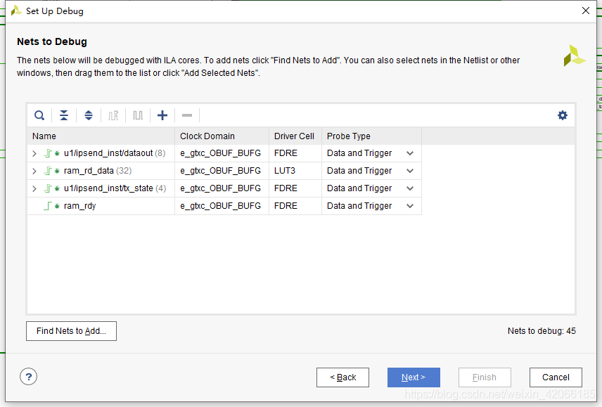
果然我的监测对象里面有这个setup debug (但是我之前这样已经下载下去过,以前是可以正常运行的,但是不知道为什么现在就不行了)
(3) 整个流程重新走一下
重新走流程
删除所有的限制文件中相关ila的内容
重新run synthesis
run 之后reload 的design
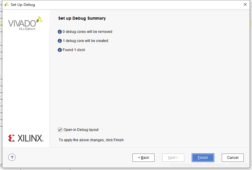
重新设定setup debug
(1) 时钟统一

(2) 需要触发功能
(3) summery 的结果
run impletmentation 和 generate
上板子调试结果如下:
减少报错的位置ram_rd_data的ila监测
此时,既然此处报错,我们选择去掉ila监测的报错情况。
重新进行编译,综合,并下载到电路板上的结果如下:
我们可以可以进入debug core:


 2万+
2万+


 被折叠的 条评论
为什么被折叠?
被折叠的 条评论
为什么被折叠?
 到【灌水乐园】发言


