


本文分析的是4K mips的内存管理,其他mips型号可能会有所区别
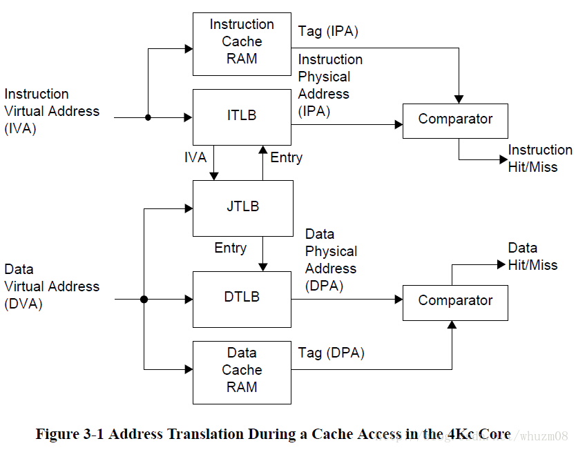
The MMU in a 4K processor core will translate any virtual address to a physical address before a request is sent to the
cache controllers for tag comparison or to the bus interface unit for an external memory reference. This translation is a
very useful feature for operating systems when trying to manage physical memory to accommodate multiple tasks active
in the same memory, possibly on the same virtual address but of course in different locations in physical memory (4Kc
core only). Other features handled by the MMU are protection of memory areas and defining the cache protocol.
In the 4Kc processor core, theMMUis TLB based. The TLB consists of three address translation buffers: a 16 dual-entry
fully associative
Joint TLB (JTLB)
, a 3-entry instruction micro
TLB (ITLB)
, and a 3-entry data micro
TLB (DTLB)
.
When an address is translated, the appropriate micro TLB (ITLB or DTLB) is accessed first. If the translation is not
found in the micro TLB, the JTLB is accessed. If there is a miss in the JTLB, an exception is taken.
BIU: bus interface unit, 这里出来的是物理地址
MMU: memory manage unit 内存管理单元
TLB: table lookup buffer
mips的内存管理方式:虚拟地址VA经过MMU,MMU查询TLB进行转换为PA,整个转换的过程不需要访问内存,所以mips的VA到PA的转换很快。
缺点是TLB的大小有限,如果TLB查询不到,就会引发TLB 异常,而频繁的异常处理会浪费大量的时间。
mips的物理地址空间分布:
#ifdef CONFIG_BRCM_HAS_1GB_MEMC0
/*
Physical address map for <= 1GB MEMC0
*
* 0000_0000 - 0fff_ffff: MEMC0 (256MB)
* 1000_0000 - 1fff_ffff: EBI/Registers (256MB), 其中 (0x1FC0_0000-1fff_ffff) 为Rom(4M)
* 2000_0000 - 4fff_ffff: MEMC0 (768MB)
* 6000_0000 - 7fff_ffff: MEMC1 (512MB)
* a000_0000 - bfff_ffff: PCIe MEM BARs (512MB)
* d000_0000 - efff_ffff: PCI2.3 MEM BARs (512MB)
* f000_0000 - f05f_ffff: PCI2.3 IO BARs (6MB)
* f000_0000 - f060_000b: PCI2.3 Configuration access (12B)
* f100_0000 - f100_001f: PCIe Configuration access - 7420 only (32B)
*
* PCI2.3/PCIe inbound BAR:
*
* 0000_0000 - 0fff_ffff: MEMC0 (256MB @ 0000_0000)
* 1000_0000 - 3fff_ffff: MEMC0 (768MB @ 2000_0000)
* 4000_0000 - 7fff_ffff: MEMC1 (1024MB @ 6000_0000) (not currently implemented)
*/
#else
/*
* Physical address map for 2GB MEMC0
*
* 0000_0000 - 0fff_ffff: MEMC0 (256MB)
* 1000_0000 - 1fff_ffff: EBI/Registers (256MB) , 其中 (0x1FC0_0000-1fff_ffff) 为Rom(4M)
* 2000_0000 - 8fff_ffff: MEMC0 (1792MB)
* 9000_0000 - cfff_ffff: MEMC1 (1024MB)
* d000_0000 - efff_ffff: PCIe MEM BARs (512MB)
*
* PCIe inbound BAR:
*
* 0000_0000 - 0fff_ffff: MEMC0 (256MB @ 0000_0000)
* 1000_0000 - 7fff_ffff: MEMC0 (1792MB @ 2000_0000)
* 8000_0000 - bfff_ffff: MEMC1 (1024MB @ 9000_0000)
*/
#endif
对于MEMC0支持1G还是2G,完全由系统硬件架构决定;
上述定义可以参考arch/mips/asm/include/spaces.h文件。
mips处在不同模式下的虚拟地址空间分布:
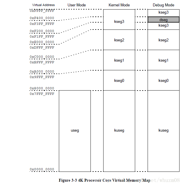
User mode is most often used for application programs. Kernel mode is typically used for handling exceptions and
privileged operating system functions, including CP0 management and I/O device accesses. Debug mode is used for
software debugging and most likely occurs within a software development tool.
The core enters Kernel mode both at reset and when an exception is recognized. While in Kernel mode, software has
access to the entire address space, as well as all CP0 registers. User mode accesses are limited to a subset of the virtual
address space (0x0000_0000 to 0x7FFF_FFFF) and can be inhibited from accessing CP0 functions. In User mode,
virtual addresses 0x8000_0000 to 0xFFFF_FFFF are invalid and cause an exception if accessed.
Debug mode is entered on a debug exception. While in Debug mode, the debug software has access to the same address
space and CP0 registers as for Kernel mode. In addition, while in Debug mode the core has access to the debug segment
dseg. This area overlays part of the kernel segment kseg3. dseg access in Debug mode can be turned on or off, allowing
full access to the entire kseg3 in Debug mode, if so desired.
Unmapped Segments
Unmapped segments have a fixed simple translation from virtual to physical address.
Except for kseg0, unmapped segments are always uncached. The cacheability of kseg0 is set in the K0 field of the CP0
register
Config
Mapped Segments
A mapped segment does use the TLB to translate from virtual to physical
address.
For the 4Kc core, the translation of mapped segments is handled on a per-page basis. Included in this translation is
information defining whether the page is cacheable or not, and the protection attributes that apply to the page
- User Mode
In user mode, a single 2 GByte (2
31
bytes) uniform virtual address space called the user segment (useg) is available.
The processor operates in User mode when the
Status
register contains the following bit values:
• UM = 1
• EXL = 0
• ERL = 0
In addition to the above values, the DM bit in the
Debug
register must be 0.
- Kernel Mode
The processor operates in Kernel mode when the DM bit in the
Debug
register is 0 and the
Status
register contains one
or more of the following values:
• UM = 0
• ERL = 1
• EXL = 1
When a non-debug exception is detected, EXL or ERL will be set and the processor will enter Kernel mode. At the end
of the exception handler routine, an Exception Return (ERET) instruction is generally executed. The ERET instruction
jumps to the Exception PC, clears ERL, and clears EXL if ERL=0. This may return the processor to User mode.
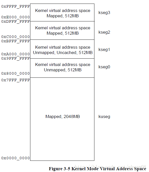
Kernel Mode, User Space (kuseg)
In Kernel mode, when the most-significant bit of the virtual address (A31) is cleared, the 32-bit kuseg virtual address
space is selected and covers the full 2
31
bytes (2 GByte) of the current user address space mapped
to addresses
0x0000_0000 - 0x7FFF_FFFF.
For the 4Kc core, the virtual address is extended with the contents of the 8-bit ASID field
to form a unique virtual address.
When ERL = 1 in the
Status
register, the user address region becomes a 2
31
-byte unmapped and uncached address space.
While in this setting, the kuseg virtual address maps directly to the same physical address, and does not include the ASID
field
.
Kernel Mode, Kernel Space 0 (kseg0)
In Kernel mode, when the most-significant three bits of the virtual address are 100
2
, 32-bit kseg0 virtual address space
is selected; it is the 2
29
-byte (512-MByte) kernel virtual space located at addresses 0x8000_0000 - 0x9FFF_FFFF.
References to kseg0 are unmapped; the physical address selected is defined by subtracting 0x8000_0000 from the virtual
address. The K0 field of the
Config
register controls cacheability.
Kernel Mode, Kernel Space 1 (kseg1)
In Kernel mode, when the most-significant three bits of the 32-bit virtual address are 101
2
, 32-bit kseg1 virtual address
space is selected. kseg1 is the 2
29
-byte (512-MByte) kernel virtual space located at addresses 0xA000_0000 -
0xBFFF_FFFF. References to kseg1 are unmapped; the physical address selected is defined by subtracting
0xA000_0000 from the virtual address. Caches are disabled for accesses to these addresses, and physical memory (or
memory-mapped I/O device registers) are accessed directly.
Kernel Mode, Kernel Space 2 (kseg2)
In Kernel mode, when UM = 0, ERL = 1, or EXL = 1 in the
Status
register, and DM = 0 in the
Debug
register, and the
most-significant three bits of the 32-bit virtual address are 110
2
, 32-bit kseg2 virtual address space is selected. This
2
29
-byte (512-MByte) kernel virtual space is located at physical addresses 0xC000_0000 - 0xDFFF_FFFF.
This space is mapped through the TLB in the 4Kc processor core.
Kernel Mode, Kernel Space 3 (kseg3)
In Kernel mode, when the most-significant three bits of the 32-bit virtual address are 1112, the kseg3 virtual address
space is selected. This 2
29
-byte (512-MByte) kernel virtual space is located at physical addresses 0xE000_0000 -
0xFFFF_FFFF. This space is mapped through the TLB in the 4Kc processor core.
正常来说映射关系为:
/*
* 256MB standard MIPS32 virtual address map
*
* 8000_0000 - 8fff_ffff: lower 256MB, cached mapping (kseg0)
* 9000_0000 - 9fff_ffff: EBI/registers, cached mapping (unused) (kseg0)
* a000_0000 - afff_ffff: lower 256MB, uncached mapping (kseg1)
* b000_0000 - bfff_ffff: EBI/registers, uncached mapping (kseg1)
* c000_0000 - ff1f_7fff: vmalloc region
* ff1f_8000 - ff1f_ffff: FIXMAP
*/
Kseg0 和Kseg1 一般来说是这样映射到物理地址0-512M,但是对于有些mips cpu可能实现配置成其他的方式,比如bmips4380,如果打开XKS01支持,则Kseg0可支持1024M,这时的映射关闭变为
:
/*
* 1024MB Broadcom 256+768 virtual address map
*
* 8000_0000 - 8fff_ffff: 256MB RAM @ 0000_0000, cached (kseg0)
* 9000_0000 - 9fff_ffff: 256MB EBI/Registers @ 1000_0000, uncached (kseg0)
* a000_0000 - cfff_ffff: 768MB RAM @ 2000_0000, cached (kseg0)
* d000_0000 - dfff_ffff: TBD
* e000_0000 - ff1f_7fff: vmalloc region
* ff1f_8000 - ff1f_ffff: FIXMAP
* ff40_0000 - ff7f_ffff: CONSISTENT region
*
* PA 5000_0000 and above are accessed through HIGHMEM (BMIPS5000 only).
*/
此时通过Kseg1访问寄存器时要特别小心,因为b000_0000 - bfff_ffff这时映射到的是DRAM而不是寄存器空间,所以想要通过这段地址空间访问寄存器之前要disable XKS01
打开XKS01的方式:
/***********************************************************************
* XKS01 support
* Certain CPUs support extending kseg0 to 1024MB.
***********************************************************************/
__CPUINIT
LEAF(bmips_enable_xks01)
#if defined(CONFIG_XKS01)
#if defined(CONFIG_CPU_BMIPS4380)
mfc0 t0, $22, 3
li t1, 0x1ff0
li t2, (1 << 12) | (1 << 9)
or t0, t1
xor t0, t1
or t0, t2
mtc0 t0, $22, 3
BARRIER
#elif defined(CONFIG_CPU_BMIPS5000)
mfc0 t0, $22, 5
li t1, 0x01ff
li t2, (1 << 8) | (1 << 5)
or t0, t1
xor t0, t1
or t0, t2
mtc0 t0, $22, 5
BARRIER
#else
#error Missing XKS01 setup
#endif
关闭XKS01的方式:
/* disable XKS01 so that CFE can access the registers */
#if defined(CONFIG_CPU_BMIPS4380)
__write_32bit_c0_register($22, 3,
__read_32bit_c0_register($22, 3) & ~BIT(12));
#elif defined(CONFIG_CPU_BMIPS5000)
__write_32bit_c0_register($22, 5,
__read_32bit_c0_register($22, 5) & ~BIT(8));
#endif
通过XKS01机制,可以在不需要TLB的情况下访问1G的物理内存:256M DRAM + 256M register + 768M DRAM
- Debug Mode
Debug mode address space is identical to Kernel mode address space with respect to mapped and unmapped areas,
except for kseg3. In kseg3, a debug segment dseg co-exists in the virtual address range 0xFF20_0000 to 0xFF3F_FFFF.
TLB填充过程

several CP0 registers must be updated with the
information to be written to a TLB entry.
• PageMask is set in the
CP0
PageMask
register
.
• VPN2 and ASID are set in the
CP0
EntryHi
register
.
• PFN0, C0, D0, V0 and G bit are set in the
CP0
EntryLo0
register.
• PFN1, C1, D1, V1 and G bit are set in the
CP0
EntryLo1
register.
并通过tlbwr或tlbwi指令把这个入口拷贝到TLB适当位置而设置起来的。
当您在处理一个TLB重装异常时,您会发现EntryHi的內容已经为您设置好了。
请当心不要创建2个匹配同一个“地址 / ASID”组合的入口。如果TLB包含重复的入口,试图转译这个地址或查找这个地址潜在上有破坏CPU芯片的可能。有些CPU在这些情形下通过关闭TLB來保护自己,表现为SR(TS)位被置起。从此时开始直到硬件重启前,TLB不会进行任何匹配。
The 4Kc core implements a TLB write-compare mechanism to ensure that multiple TLB matches do not occur. On the
TLB write operation, the VPN2 field to be written is compared with all other entries in the TLB. If a match occurs, the
4Kc core takes a machine-check exception, sets the TS bit in the CP0
Status
register, and aborts the write operation.
There is a hidden bit in each TLB entry
that is cleared on a ColdReset. This bit is set once the TLB entry is written and is included in the match detection.
Therefore, uninitialized TLB entries will not cause a TLB shutdown.
Note: This hidden initialization bit leaves the entire JTLB invalid after a ColdReset, eliminating the need to flush the
TLB. But, to be compatible with other MIPS processors, it is recommended that software initialize all TLB entries with
unique tag values and V bits cleared before the first access to a mapped location.
系统软件通常根本不需要读TLB入口。不过如果您想读它们,可以使用tlbp指令來查找一个装有特定地址的TLB入口,并看到结果反映在Index寄存器。不要忘记先保存好EntryHi寄存器并在查找之后重新恢复它,因为它的ASID域是很重要的。
您可以使用tlbr来读取TLB入口中的內容到EntryHi和EntryLo中去。
您可以发现CPU的文档中为了进行对指令和数据地址的转译而把TLB结构划分成ITLB和DTLB;这些都是微小的硬件控制快存,它们的操作对软件是完全透明的。
使用ASID
我们通过一个专门的ASID配置和把EntryLo的G位设置为0来建立TLB入口,除非CPU的EntryHi(ASID)寄存器域与TLB入口的相应值相符,那些入口是永远不会与一个程序地址完全匹配的。这就允许你同时映射64或256个不同的地址空间,而不需要在进程切换时完全清除TLB。
对于一个多任务操作系统来讲,每个任务都有 自己的4G虚拟空间,但是有自己的ASID。 通过ASID,CPU可以区分两个具有同样虚拟地址的TLB其实是分别属于不同的操作系统的 进程或任务。
相关寄存器:
注意区分TLB entrys中的字段bit和CP0 相关寄存器中字段的不同,我们需要关注的是寄存器中的字段
Entry Hi
Entry Hi寄存器存放VPN2,或一个TLB的虚拟地址部分。
A TLB exception (TLB Refill, TLB Invalid, or TLB Modified) causes bits VA31:13 of the virtual address to be written
into the VPN2 field of the
EntryHi
register. The ASID field is written by software with the current address space
identifier value and is used during the TLB comparison process to determine TLB match.

G:Global Bit. When set, indicates that this entry is global to all processes and/or
threads and thus disables inclusion of the ASID in the comparison. ASID[7:0]:Address Space Identifier. Identifies which process or thread this TLB entry is
associated with.
Page Mask
MIPS TLB提供可变大小的TLB地址映射。一个页面可以是4K,16K,64K,256K,1M,4M或16M。这种可变页大小(PAGE SIZE)提供了很好的 灵活性,特别是对嵌入式系统软件。 对于嵌入式应用,一个很大的区别就是:不允许大 量的页面错处理。否则系统性能 将会非常的差。这一点与传统意义上的操作系统是不一 样的。传统OS存储管理的一个原则就是:Page On
Demand。这对大多嵌入式系统是不允许的。 嵌入式系统往往是需要在系统初始化的时刻 就对所有的存储进行配置,以确保在系统运行时不会有页面错异常。

Page Mask Value. The Page Mask defines the page size by masking the
appropriate VPN2 bits from being involved in a comparison. It is also used to
determine which address bit is used to make the even-odd page (PFN0-PFN1)
determination. See the table below.

The PageMask column above show all the legal values for PageMask. Because
each pair of bits can only have the same value, the physical entry in the JTLB
will only save a compressed version of the PageMask using only 6 bits. This is
however transparent to software, which will always work with a 12 bit field.
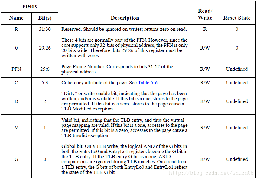
EntryLo0, EntryLo1
这两个寄存器是用来指定 一个TLB 对的偶(even)和奇(odd)物理(Physical)页面地址。
一定要注意的是:EntryLo0是给偶数TLB页面, EntryLo1是给奇数TLB页面使用的。否 则MMU会报异常错误。通常是系统不能启动。


对于bmips4380:
#define K_CALG_COH_EXCL1_NOL2 0
#define K_CALG_COH_SHRL1_NOL2 1
#define K_CALG_UNCACHED 2
#define K_CALG_NONCOHERENT 3
#define K_CALG_COH_EXCL 4
#define K_CALG_COH_SHAREABLE 5
#define K_CALG_NOTUSED 6
#define K_CALG_UNCACHED_ACCEL 7
Random
register
The Random
register selects which TLB entry to use on a TLBWR. This register decrements almost every cycle, wrapping to the
maximum once it’s value is equal to the
Wired
register. Thus, TLB entries below the
Wired
value cannot be replaced by
a TLBWR allowing important mappings to be preserved. In order to reduce the possibility for a livelock situation, the
Random
register includes a 10b LFSR that introduces a pseudo-random perturbation into the decrementing.
The
Random
register is a read-only register. The value of the register varies between an upper and lower bound as follow:
• A lower bound is set by the number of TLB entries reserved for exclusive use by the operating system (the contents
of the
Wired
register). The entry indexed by the
Wired
register is the first entry available to be written by a TLB Write
Random operation.
• An upper bound is set by the total number of TLB entries minus 1.


Wired register
the processor provides a mechanism whereby a programmable number of mappings can be locked into the TLB via the CP0 Wired register, thus avoiding random replacement.
The
Wired
register is a read/write register

index register
TLBWI指令根据index register写对应的TLB入口,
The
Index
register is a 32-bit read/write register

The operation of the processor is UNDEFINED if a value greater than or equal to the number of TLB entries is written
to the
Index
register.
P:Probe Failure. Set to 1 when the previous TLBProbe (TLBP) instruction failed to find a match in the TLB.
Context Register
该寄存器主要是为TLB异常提供额外信息,可加快TLB异常处理的速度
The
Context
register is a read/write register containing a pointer to an entry in the page table entry (PTE) array. This
array is an operating system data structure that stores virtual-to-physical translations. During a TLB miss, the operating
system loads the TLB with the missing translation from the PTE array. The
Context
register duplicates some of the
information provided in the
BadVAddr
register but is organized in such a way that the operating system can directly
reference an 8-byte page table entry (PTE) in memory.
A TLB exception (TLB Refill, TLB Invalid, or TLB Modified) causes bits VA
31:13
of the virtual address to be written
into the BadVPN2 field of the
Context
register.
The PTEBase field is written and used by the operating system.
The BadVPN2 field of the
Context
register is not defined after an address error exception.


Instruction TLB
The ITLB is a small 3-entry, fully associative TLB dedicated to performing translations for the instruction stream. The
ITLB only maps 4-Kbyte pages/sub-pages.
The ITLB is managed by hardware and is transparent to software. If a fetch address cannot be translated by the ITLB,
the JTLB is accessed to attempt to translate it in the following clock cycle. If successful, the translation information is
copied into the ITLB. The ITLB is then re-accessed and the address will be successfully translated. This results in an
ITLB miss penalty of at least 2 cycles (if the JTLB is busy with other operations, it may take additional cycles).
Data TLB
The DTLB is a small 3-entry, fully associative TLB which provides a faster translation for Load/Store addresses than is
possible with the JTLB. The DTLB only maps 4-Kbyte pages/sub-pages.
Like the ITLB, the DTLB is managed by hardware and is transparent to software. Unlike the ITLB, when translating
Load/Store addresses, the JTLB is accessed in parallel with the DTLB. If there is a DTLB miss and a JTLB hit, the DTLB
can be reloaded that cycle. The DTLB is then re-accessed and the translation will be successful. This parallel access
reduces the DTLB miss penalty to 1 cycle.
TLB转换过程
当前的进程的ASID是保存在哪来的呢
可以参考switch_mm()函数
static inline void switch_mm(struct mm_struct *prev, struct mm_struct *next,
struct task_struct *tsk)
{
unsigned int cpu = smp_processor_id();
unsigned long flags;
local_irq_save(flags);
/* Check if our ASID is of an older version and thus invalid */
if ((cpu_context(cpu, next) ^ asid_cache(cpu)) & ASID_VERSION_MASK)
get_new_mmu_context(next, cpu);
write_c0_entryhi(cpu_asid(cpu, next));
TLBMISS_HANDLER_SETUP_PGD(next->pgd);
/*
* Mark current->active_mm as not "active" anymore.
* We don't want to mislead possible IPI tlb flush routines.
*/
cpumask_clear_cpu(cpu, mm_cpumask(prev));
cpumask_set_cpu(cpu, mm_cpumask(next));
local_irq_restore(flags);
}
因此当前进程的ASID是设置在
Entry Hi寄存器中的

代码分析:
cfe中关于TLB部分的代码:
LEAF(init_tlb)
.set noreorder
/*********************************************************************
* Initialize all TLB entries
*********************************************************************/
/* Set page size to 4KB */
mtc0 zero, CP0_PAGE_MASK //#define CP0_PAGE_MASK $5
/* set all entries to valid=0 with unique kseg0 VAs */
li t0,
0x80000000
//kseg0 是ummap的,所以这里TLB初始只是为了不冲突
li v0, 0
li v1, 32 //NUM_TLB_ENTRIES //TLB entries 的个数
li t4, 0 //index从0开始
zero_tlb_loop:
mtc0 t0, CP0_ENTRY_HI
mtc0 zero, CP0_ENTRY_LO_0
mtc0 zero, CP0_ENTRY_LO_1
mtc0 t4, CP0_INDEX
BARRIER
tlbwi
BARRIER
addi t0,t0,0x2000
addi t4,t4,1 //index ++
addi v0,v0,1
bne v0,v1,zero_tlb_loop
nop
li t0, PM_256MB //#define PM_256MB 0x1fffe000 对应的二进制位11111111111111110000000000000 (前面16bit为1,后面13bit为0,对于mips4380,31-29:0 28-13:page mask 12-0:0, 最大一个页支持256M),表明一个页是256M
mtc0 t0, CP0_PAGE_MASK
li t0, DRAM00_VIRT_ADDR //#define DRAM00_VIRT_ADDR (0x20000000) 即512M
mtc0 t0, CP0_ENTRY_HI
//#define DRAM00_PHYS_ADDR (0x20000000)
li t0, ENTRYLO_UNCACHED(DRAM00_PHYS_ADDR)
//
#define ENTRYLO_UNCACHED(x) ((((x) >> 6) & 0x3fffffc0) | 0x17) 0x17=b0001 0111, 即 【5-3】cache=010 (uncache) 【2】D=1 【1】V=1 【0】G=1
mtc0 t0, CP0_ENTRY_LO_0
li t0, ENTRYLO_UNCACHED(DRAM00_PHYS_ADDR + OFFS_256MB) //(0x30000000)
mtc0 t0, CP0_ENTRY_LO_1
li t0, 1 //index为1
mtc0 t0, CP0_INDEX
BARRIER
tlbwi
BARRIER
li t0, PM_256MB
mtc0 t0, CP0_PAGE_MASK
li t0, DRAM01_VIRT_ADDR //#define DRAM01_VIRT_ADDR (0x40000000)
mtc0 t0, CP0_ENTRY_HI
li t0, ENTRYLO_UNCACHED(DRAM01_PHYS_ADDR) //#define DRAM01_PHYS_ADDR (0x40000000)
mtc0 t0, CP0_ENTRY_LO_0
li t0, ENTRYLO_UNCACHED(DRAM01_PHYS_ADDR + OFFS_256MB)
mtc0 t0, CP0_ENTRY_LO_1
li t0, 2 //index为2
mtc0 t0, CP0_INDEX
BARRIER
tlbwi
BARRIER
li t0, PM_256MB
mtc0 t0, CP0_PAGE_MASK
li t0, DRAM02_VIRT_ADDR //#define DRAM02_VIRT_ADDR (0x60000000)
mtc0 t0, CP0_ENTRY_HI
li t0, ENTRYLO_UNCACHED(DRAM02_PHYS_ADDR)
mtc0 t0, CP0_ENTRY_LO_0
li t0, ENTRYLO_UNCACHED(DRAM02_PHYS_ADDR + OFFS_256MB)
mtc0 t0, CP0_ENTRY_LO_1
li t0, 3 //index为3
mtc0 t0, CP0_INDEX
BARRIER
tlbwi
BARRIER
/* map virtual address range 0x00000000-0x1fffffff to physical address range 0x00000000-0x1fffffff.
* This is needed for S3 warmboot when linux uses lower memory.
*/
li t0, PM_256MB
mtc0 t0, CP0_PAGE_MASK
li t0, DRAM03_VIRT_ADDR // #define DRAM03_VIRT_ADDR (0x00000000)
mtc0 t0, CP0_ENTRY_HI
li t0, ENTRYLO_UNCACHED(DRAM03_PHYS_ADDR) //#define DRAM03_PHYS_ADDR (0x00000000)
mtc0 t0, CP0_ENTRY_LO_0
li t0, ENTRYLO_UNCACHED(DRAM03_PHYS_ADDR + OFFS_256MB)
mtc0 t0, CP0_ENTRY_LO_1
li t0, 4 //index为4
mtc0 t0, CP0_INDEX
BARRIER
tlbwi
BARRIER
li t0, 5 //设置wired =5,也就是刚才设置的TLB entries不被tlbwr指令覆盖
mtc0 t0, CP0_WIRED
.set reorder
jr ra
nop
END(init_tlb)
也就是说在cfe中Kuseg是可以访问的, 虚拟地址空间0x7ffff_ffff - 0x0000_0000直接映射到物理地址空间0x7ffff_ffff - 0x0000_0000,是uncache的
注意上面entry lo寄存器的设置中PFN的设置
//
#define ENTRYLO_UNCACHED(x) ((((x) >> 6) & 0x3fffffc0) | 0x17) 其中x是映射到的物理地址


 2万+
2万+

 被折叠的 条评论
为什么被折叠?
被折叠的 条评论
为什么被折叠?
 到【灌水乐园】发言


