


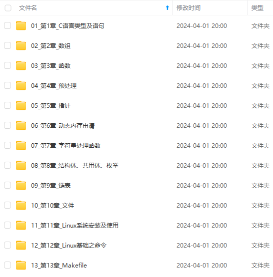
既有适合小白学习的零基础资料,也有适合3年以上经验的小伙伴深入学习提升的进阶课程,涵盖了95%以上C C++开发知识点,真正体系化!
由于文件比较多,这里只是将部分目录截图出来,全套包含大厂面经、学习笔记、源码讲义、实战项目、大纲路线、讲解视频,并且后续会持续更新
- This register stores the data to be written into the Slave 4. If I2C_SLV4_RW
- is set 1 (set to read), this register has no effect.
- @param data New byte to write to Slave 4
- @see MPU6500_RA_I2C_SLV4_DO
/
void mpu6500SetSlave4OutputByte(uint8_t data)
{
i2cdevWriteByte(I2Cx, devAddr, MPU6500_RA_I2C_SLV4_DO, data);
}
/* Get the enabled value for the Slave 4. - When set to 1, this bit enables Slave 4 for data transfer operations. When
- cleared to 0, this bit disables Slave 4 from data transfer operations.
- @return Current enabled value for Slave 4
- @see MPU6500_RA_I2C_SLV4_CTRL
/
bool mpu6500GetSlave4Enabled()
{
i2cdevReadBit(I2Cx, devAddr, MPU6500_RA_I2C_SLV4_CTRL, MPU6500_I2C_SLV4_EN_BIT, buffer);
return buffer[0];
}
/* Set the enabled value for Slave 4. - @param enabled New enabled value for Slave 4
- @see getSlave4Enabled()
- @see MPU6500_RA_I2C_SLV4_CTRL
/
void mpu6500SetSlave4Enabled(bool enabled)
{
i2cdevWriteBit(I2Cx, devAddr, MPU6500_RA_I2C_SLV4_CTRL, MPU6500_I2C_SLV4_EN_BIT, enabled);
}
/* Get the enabled value for Slave 4 transaction interrupts. - When set to 1, this bit enables the generation of an interrupt signal upon
- completion of a Slave 4 transaction. When cleared to 0, this bit disables the
- generation of an interrupt signal upon completion of a Slave 4 transaction.
- The interrupt status can be observed in Register 54.
- @return Current enabled value for Slave 4 transaction interrupts.
- @see MPU6500_RA_I2C_SLV4_CTRL
/
bool mpu6500GetSlave4InterruptEnabled()
{
i2cdevReadBit(I2Cx, devAddr, MPU6500_RA_I2C_SLV4_CTRL, MPU6500_I2C_SLV4_INT_EN_BIT, buffer);
return buffer[0];
}
/* Set the enabled value for Slave 4 transaction interrupts. - @param enabled New enabled value for Slave 4 transaction interrupts.
- @see getSlave4InterruptEnabled()
- @see MPU6500_RA_I2C_SLV4_CTRL
/
void mpu6500SetSlave4InterruptEnabled(bool enabled)
{
i2cdevWriteBit(I2Cx, devAddr, MPU6500_RA_I2C_SLV4_CTRL, MPU6500_I2C_SLV4_INT_EN_BIT, enabled);
}
/* Get write mode for Slave 4. - When set to 1, the transaction will read or write data only. When cleared to
- 0, the transaction will write a register address prior to reading or writing
- data. This should equal 0 when specifying the register address within the
- Slave device to/from which the ensuing data transaction will take place.
- @return Current write mode for Slave 4 (0 = register address + data, 1 = data only)
- @see MPU6500_RA_I2C_SLV4_CTRL
/
bool mpu6500GetSlave4WriteMode()
{
i2cdevReadBit(I2Cx, devAddr, MPU6500_RA_I2C_SLV4_CTRL, MPU6500_I2C_SLV4_REG_DIS_BIT, buffer);
return buffer[0];
}
/* Set write mode for the Slave 4. - @param mode New write mode for Slave 4 (0 = register address + data, 1 = data only)
- @see getSlave4WriteMode()
- @see MPU6500_RA_I2C_SLV4_CTRL
/
void mpu6500SetSlave4WriteMode(bool mode)
{
i2cdevWriteBit(I2Cx, devAddr, MPU6500_RA_I2C_SLV4_CTRL, MPU6500_I2C_SLV4_REG_DIS_BIT, mode);
}
/* Get Slave 4 master delay value. - This configures the reduced access rate of I2C slaves relative to the Sample
- Rate. When a slave’s access rate is decreased relative to the Sample Rate,
- the slave is accessed every:
-
1 / (1 + I2C_MST_DLY) samples - This base Sample Rate in turn is determined by SMPLRT_DIV (register 25) and
- DLPF_CFG (register 26). Whether a slave’s access rate is reduced relative to
- the Sample Rate is determined by I2C_MST_DELAY_CTRL (register 103). For
- further information regarding the Sample Rate, please refer to register 25.
- @return Current Slave 4 master delay value
- @see MPU6500_RA_I2C_SLV4_CTRL
/
uint8_t mpu6500GetSlave4MasterDelay()
{
i2cdevReadBits(I2Cx, devAddr, MPU6500_RA_I2C_SLV4_CTRL, MPU6500_I2C_SLV4_MST_DLY_BIT,
MPU6500_I2C_SLV4_MST_DLY_LENGTH, buffer);
return buffer[0];
}
/* Set Slave 4 master delay value. - @param delay New Slave 4 master delay value
- @see getSlave4MasterDelay()
- @see MPU6500_RA_I2C_SLV4_CTRL
/
void mpu6500SetSlave4MasterDelay(uint8_t delay)
{
i2cdevWriteBits(I2Cx, devAddr, MPU6500_RA_I2C_SLV4_CTRL, MPU6500_I2C_SLV4_MST_DLY_BIT,
MPU6500_I2C_SLV4_MST_DLY_LENGTH, delay);
}
/* Get last available byte read from Slave 4. - This register stores the data read from Slave 4. This field is populated
- after a read transaction.
- @return Last available byte read from to Slave 4
- @see MPU6500_RA_I2C_SLV4_DI
*/
uint8_t mpu6500GetSlate4InputByte()
{
i2cdevReadByte(I2Cx, devAddr, MPU6500_RA_I2C_SLV4_DI, buffer);
return buffer[0];
}
// I2C_MST_STATUS register
/** Get FSYNC interrupt status.
- This bit reflects the status of the FSYNC interrupt from an external device
- into the MPU-60X0. This is used as a way to pass an external interrupt
- through the MPU-60X0 to the host application processor. When set to 1, this
- bit will cause an interrupt if FSYNC_INT_EN is asserted in INT_PIN_CFG
- (Register 55).
- @return FSYNC interrupt status
- @see MPU6500_RA_I2C_MST_STATUS
/
bool mpu6500GetPassthroughStatus()
{
i2cdevReadBit(I2Cx, devAddr, MPU6500_RA_I2C_MST_STATUS, MPU6500_MST_PASS_THROUGH_BIT, buffer);
return buffer[0];
}
/* Get Slave 4 transaction done status. - Automatically sets to 1 when a Slave 4 transaction has completed. This
- triggers an interrupt if the I2C_MST_INT_EN bit in the INT_ENABLE register
- (Register 56) is asserted and if the SLV_4_DONE_INT bit is asserted in the
- I2C_SLV4_CTRL register (Register 52).
- @return Slave 4 transaction done status
- @see MPU6500_RA_I2C_MST_STATUS
/
bool mpu6500GetSlave4IsDone()
{
i2cdevReadBit(I2Cx, devAddr, MPU6500_RA_I2C_MST_STATUS, MPU6500_MST_I2C_SLV4_DONE_BIT, buffer);
return buffer[0];
}
/* Get master arbitration lost status. - This bit automatically sets to 1 when the I2C Master has lost arbitration of
- the auxiliary I2C bus (an error condition). This triggers an interrupt if the
- I2C_MST_INT_EN bit in the INT_ENABLE register (Register 56) is asserted.
- @return Master arbitration lost status
- @see MPU6500_RA_I2C_MST_STATUS
/
bool mpu6500GetLostArbitration()
{
i2cdevReadBit(I2Cx, devAddr, MPU6500_RA_I2C_MST_STATUS, MPU6500_MST_I2C_LOST_ARB_BIT, buffer);
return buffer[0];
}
/* Get Slave 4 NACK status. - This bit automatically sets to 1 when the I2C Master receives a NACK in a
- transaction with Slave 4. This triggers an interrupt if the I2C_MST_INT_EN
- bit in the INT_ENABLE register (Register 56) is asserted.
- @return Slave 4 NACK interrupt status
- @see MPU6500_RA_I2C_MST_STATUS
/
bool mpu6500GetSlave4Nack()
{
i2cdevReadBit(I2Cx, devAddr, MPU6500_RA_I2C_MST_STATUS, MPU6500_MST_I2C_SLV4_NACK_BIT, buffer);
return buffer[0];
}
/* Get Slave 3 NACK status. - This bit automatically sets to 1 when the I2C Master receives a NACK in a
- transaction with Slave 3. This triggers an interrupt if the I2C_MST_INT_EN
- bit in the INT_ENABLE register (Register 56) is asserted.
- @return Slave 3 NACK interrupt status
- @see MPU6500_RA_I2C_MST_STATUS
/
bool mpu6500GetSlave3Nack()
{
i2cdevReadBit(I2Cx, devAddr, MPU6500_RA_I2C_MST_STATUS, MPU6500_MST_I2C_SLV3_NACK_BIT, buffer);
return buffer[0];
}
/* Get Slave 2 NACK status. - This bit automatically sets to 1 when the I2C Master receives a NACK in a
- transaction with Slave 2. This triggers an interrupt if the I2C_MST_INT_EN
- bit in the INT_ENABLE register (Register 56) is asserted.
- @return Slave 2 NACK interrupt status
- @see MPU6500_RA_I2C_MST_STATUS
/
bool mpu6500GetSlave2Nack()
{
i2cdevReadBit(I2Cx, devAddr, MPU6500_RA_I2C_MST_STATUS, MPU6500_MST_I2C_SLV2_NACK_BIT, buffer);
return buffer[0];
}
/* Get Slave 1 NACK status. - This bit automatically sets to 1 when the I2C Master receives a NACK in a
- transaction with Slave 1. This triggers an interrupt if the I2C_MST_INT_EN
- bit in the INT_ENABLE register (Register 56) is asserted.
- @return Slave 1 NACK interrupt status
- @see MPU6500_RA_I2C_MST_STATUS
/
bool mpu6500GetSlave1Nack()
{
i2cdevReadBit(I2Cx, devAddr, MPU6500_RA_I2C_MST_STATUS, MPU6500_MST_I2C_SLV1_NACK_BIT, buffer);
return buffer[0];
}
/* Get Slave 0 NACK status. - This bit automatically sets to 1 when the I2C Master receives a NACK in a
- transaction with Slave 0. This triggers an interrupt if the I2C_MST_INT_EN
- bit in the INT_ENABLE register (Register 56) is asserted.
- @return Slave 0 NACK interrupt status
- @see MPU6500_RA_I2C_MST_STATUS
*/
bool mpu6500GetSlave0Nack()
{
i2cdevReadBit(I2Cx, devAddr, MPU6500_RA_I2C_MST_STATUS, MPU6500_MST_I2C_SLV0_NACK_BIT, buffer);
return buffer[0];
}
// INT_PIN_CFG register
/** Get interrupt logic level mode.
- Will be set 0 for active-high, 1 for active-low.
- @return Current interrupt mode (0=active-high, 1=active-low)
- @see MPU6500_RA_INT_PIN_CFG
- @see MPU6500_INTCFG_INT_LEVEL_BIT
/
bool mpu6500GetInterruptMode()
{
i2cdevReadBit(I2Cx, devAddr, MPU6500_RA_INT_PIN_CFG, MPU6500_INTCFG_INT_LEVEL_BIT, buffer);
return buffer[0];
}
/* Set interrupt logic level mode. - @param mode New interrupt mode (0=active-high, 1=active-low)
- @see getInterruptMode()
- @see MPU6500_RA_INT_PIN_CFG
- @see MPU6500_INTCFG_INT_LEVEL_BIT
/
void mpu6500SetInterruptMode(bool mode)
{
i2cdevWriteBit(I2Cx, devAddr, MPU6500_RA_INT_PIN_CFG, MPU6500_INTCFG_INT_LEVEL_BIT, mode);
}
/* Get interrupt drive mode. - Will be set 0 for push-pull, 1 for open-drain.
- @return Current interrupt drive mode (0=push-pull, 1=open-drain)
- @see MPU6500_RA_INT_PIN_CFG
- @see MPU6500_INTCFG_INT_OPEN_BIT
/
bool mpu6500GetInterruptDrive()
{
i2cdevReadBit(I2Cx, devAddr, MPU6500_RA_INT_PIN_CFG, MPU6500_INTCFG_INT_OPEN_BIT, buffer);
return buffer[0];
}
/* Set interrupt drive mode. - @param drive New interrupt drive mode (0=push-pull, 1=open-drain)
- @see getInterruptDrive()
- @see MPU6500_RA_INT_PIN_CFG
- @see MPU6500_INTCFG_INT_OPEN_BIT
/
void mpu6500SetInterruptDrive(bool drive)
{
i2cdevWriteBit(I2Cx, devAddr, MPU6500_RA_INT_PIN_CFG, MPU6500_INTCFG_INT_OPEN_BIT, drive);
}
/* Get interrupt latch mode. - Will be set 0 for 50us-pulse, 1 for latch-until-int-cleared.
- @return Current latch mode (0=50us-pulse, 1=latch-until-int-cleared)
- @see MPU6500_RA_INT_PIN_CFG
- @see MPU6500_INTCFG_LATCH_INT_EN_BIT
/
bool mpu6500GetInterruptLatch()
{
i2cdevReadBit(I2Cx, devAddr, MPU6500_RA_INT_PIN_CFG, MPU6500_INTCFG_LATCH_INT_EN_BIT, buffer);
return buffer[0];
}
/* Set interrupt latch mode. - @param latch New latch mode (0=50us-pulse, 1=latch-until-int-cleared)
- @see getInterruptLatch()
- @see MPU6500_RA_INT_PIN_CFG
- @see MPU6500_INTCFG_LATCH_INT_EN_BIT
/
void mpu6500SetInterruptLatch(bool latch)
{
i2cdevWriteBit(I2Cx, devAddr, MPU6500_RA_INT_PIN_CFG, MPU6500_INTCFG_LATCH_INT_EN_BIT, latch);
}
/* Get interrupt latch clear mode. - Will be set 0 for status-read-only, 1 for any-register-read.
- @return Current latch clear mode (0=status-read-only, 1=any-register-read)
- @see MPU6500_RA_INT_PIN_CFG
- @see MPU6500_INTCFG_INT_RD_CLEAR_BIT
/
bool mpu6500GetInterruptLatchClear()
{
i2cdevReadBit(I2Cx, devAddr, MPU6500_RA_INT_PIN_CFG, MPU6500_INTCFG_INT_RD_CLEAR_BIT, buffer);
return buffer[0];
}
/* Set interrupt latch clear mode. - @param clear New latch clear mode (0=status-read-only, 1=any-register-read)
- @see getInterruptLatchClear()
- @see MPU6500_RA_INT_PIN_CFG
- @see MPU6500_INTCFG_INT_RD_CLEAR_BIT
/
void mpu6500SetInterruptLatchClear(bool clear)
{
i2cdevWriteBit(I2Cx, devAddr, MPU6500_RA_INT_PIN_CFG, MPU6500_INTCFG_INT_RD_CLEAR_BIT, clear);
}
/* Get FSYNC interrupt logic level mode. - @return Current FSYNC interrupt mode (0=active-high, 1=active-low)
- @see getFSyncInterruptMode()
- @see MPU6500_RA_INT_PIN_CFG
- @see MPU6500_INTCFG_FSYNC_INT_LEVEL_BIT
/
bool mpu6500GetFSyncInterruptLevel()
{
i2cdevReadBit(I2Cx, devAddr, MPU6500_RA_INT_PIN_CFG, MPU6500_INTCFG_FSYNC_INT_LEVEL_BIT, buffer);
return buffer[0];
}
/* Set FSYNC interrupt logic level mode. - @param mode New FSYNC interrupt mode (0=active-high, 1=active-low)
- @see getFSyncInterruptMode()
- @see MPU6500_RA_INT_PIN_CFG
- @see MPU6500_INTCFG_FSYNC_INT_LEVEL_BIT
/
void mpu6500SetFSyncInterruptLevel(bool level)
{
i2cdevWriteBit(I2Cx, devAddr, MPU6500_RA_INT_PIN_CFG, MPU6500_INTCFG_FSYNC_INT_LEVEL_BIT, level);
}
/* Get FSYNC pin interrupt enabled setting. - Will be set 0 for disabled, 1 for enabled.
- @return Current interrupt enabled setting
- @see MPU6500_RA_INT_PIN_CFG
- @see MPU6500_INTCFG_FSYNC_INT_EN_BIT
/
bool mpu6500GetFSyncInterruptEnabled()
{
i2cdevReadBit(I2Cx, devAddr, MPU6500_RA_INT_PIN_CFG, MPU6500_INTCFG_FSYNC_INT_EN_BIT, buffer);
return buffer[0];
}
/* Set FSYNC pin interrupt enabled setting. - @param enabled New FSYNC pin interrupt enabled setting
- @see getFSyncInterruptEnabled()
- @see MPU6500_RA_INT_PIN_CFG
- @see MPU6500_INTCFG_FSYNC_INT_EN_BIT
/
void mpu6500SetFSyncInterruptEnabled(bool enabled)
{
i2cdevWriteBit(I2Cx, devAddr, MPU6500_RA_INT_PIN_CFG, MPU6500_INTCFG_FSYNC_INT_EN_BIT, enabled);
}
/* Get I2C bypass enabled status. - When this bit is equal to 1 and I2C_MST_EN (Register 106 bit[5]) is equal to
- 0, the host application processor will be able to directly access the
- auxiliary I2C bus of the MPU-60X0. When this bit is equal to 0, the host
- application processor will not be able to directly access the auxiliary I2C
- bus of the MPU-60X0 regardless of the state of I2C_MST_EN (Register 106
- bit[5]).
- @return Current I2C bypass enabled status
- @see MPU6500_RA_INT_PIN_CFG
- @see MPU6500_INTCFG_I2C_BYPASS_EN_BIT
/
bool mpu6500GetI2CBypassEnabled()
{
i2cdevReadBit(I2Cx, devAddr, MPU6500_RA_INT_PIN_CFG, MPU6500_INTCFG_I2C_BYPASS_EN_BIT, buffer);
return buffer[0];
}
/* Set I2C bypass enabled status. - When this bit is equal to 1 and I2C_MST_EN (Register 106 bit[5]) is equal to
- 0, the host application processor will be able to directly access the
- auxiliary I2C bus of the MPU-60X0. When this bit is equal to 0, the host
- application processor will not be able to directly access the auxiliary I2C
- bus of the MPU-60X0 regardless of the state of I2C_MST_EN (Register 106
- bit[5]).
- @param enabled New I2C bypass enabled status
- @see MPU6500_RA_INT_PIN_CFG
- @see MPU6500_INTCFG_I2C_BYPASS_EN_BIT
/
void mpu6500SetI2CBypassEnabled(bool enabled)
{
i2cdevWriteBit(I2Cx, devAddr, MPU6500_RA_INT_PIN_CFG, MPU6500_INTCFG_I2C_BYPASS_EN_BIT, enabled);
}
/* Get reference clock output enabled status. - When this bit is equal to 1, a reference clock output is provided at the
- CLKOUT pin. When this bit is equal to 0, the clock output is disabled. For
- further information regarding CLKOUT, please refer to the MPU-60X0 Product
- Specification document.
- @return Current reference clock output enabled status
- @see MPU6500_RA_INT_PIN_CFG
- @see MPU6500_INTCFG_CLKOUT_EN_BIT
/
bool mpu6500GetClockOutputEnabled()
{
i2cdevReadBit(I2Cx, devAddr, MPU6500_RA_INT_PIN_CFG, MPU6500_INTCFG_CLKOUT_EN_BIT, buffer);
return buffer[0];
}
/* Set reference clock output enabled status. - When this bit is equal to 1, a reference clock output is provided at the
- CLKOUT pin. When this bit is equal to 0, the clock output is disabled. For
- further information regarding CLKOUT, please refer to the MPU-60X0 Product
- Specification document.
- @param enabled New reference clock output enabled status
- @see MPU6500_RA_INT_PIN_CFG
- @see MPU6500_INTCFG_CLKOUT_EN_BIT
*/
void mpu6500SetClockOutputEnabled(bool enabled)
{
i2cdevWriteBit(I2Cx, devAddr, MPU6500_RA_INT_PIN_CFG, MPU6500_INTCFG_CLKOUT_EN_BIT, enabled);
}
// INT_ENABLE register
/** Get full interrupt enabled status.
- Full register byte for all interrupts, for quick reading. Each bit will be
- set 0 for disabled, 1 for enabled.
- @return Current interrupt enabled status
- @see MPU6500_RA_INT_ENABLE
- @see MPU6500_INTERRUPT_FF_BIT
/
uint8_t mpu6500GetIntEnabled()
{
i2cdevReadByte(I2Cx, devAddr, MPU6500_RA_INT_ENABLE, buffer);
return buffer[0];
}
/ Set full interrupt enabled status. - Full register byte for all interrupts, for quick reading. Each bit should be
- set 0 for disabled, 1 for enabled.
- @param enabled New interrupt enabled status
- @see getIntFreefallEnabled()
- @see MPU6500_RA_INT_ENABLE
- @see MPU6500_INTERRUPT_FF_BIT
/
void mpu6500SetIntEnabled(uint8_t enabled)
{
i2cdevWriteByte(I2Cx, devAddr, MPU6500_RA_INT_ENABLE, enabled);
}
/ Get Free Fall interrupt enabled status. - Will be set 0 for disabled, 1 for enabled.
- @return Current interrupt enabled status
- @see MPU6500_RA_INT_ENABLE
- @see MPU6500_INTERRUPT_FF_BIT
/
bool mpu6500GetIntFreefallEnabled()
{
i2cdevReadBit(I2Cx, devAddr, MPU6500_RA_INT_ENABLE, MPU6500_INTERRUPT_FF_BIT, buffer);
return buffer[0];
}
/ Set Free Fall interrupt enabled status. - @param enabled New interrupt enabled status
- @see getIntFreefallEnabled()
- @see MPU6500_RA_INT_ENABLE
- @see MPU6500_INTERRUPT_FF_BIT
/
void mpu6500SetIntFreefallEnabled(bool enabled)
{
i2cdevWriteBit(I2Cx, devAddr, MPU6500_RA_INT_ENABLE, MPU6500_INTERRUPT_FF_BIT, enabled);
}
/ Get Motion Detection interrupt enabled status. - Will be set 0 for disabled, 1 for enabled.
- @return Current interrupt enabled status
- @see MPU6500_RA_INT_ENABLE
- @see MPU6500_INTERRUPT_MOT_BIT
/
bool mpu6500GetIntMotionEnabled()
{
i2cdevReadBit(I2Cx, devAddr, MPU6500_RA_INT_ENABLE, MPU6500_INTERRUPT_MOT_BIT, buffer);
return buffer[0];
}
/ Set Motion Detection interrupt enabled status. - @param enabled New interrupt enabled status
- @see getIntMotionEnabled()
- @see MPU6500_RA_INT_ENABLE
- @see MPU6500_INTERRUPT_MOT_BIT
/
void mpu6500SetIntMotionEnabled(bool enabled)
{
i2cdevWriteBit(I2Cx, devAddr, MPU6500_RA_INT_ENABLE, MPU6500_INTERRUPT_MOT_BIT, enabled);
}
/ Get Zero Motion Detection interrupt enabled status. - Will be set 0 for disabled, 1 for enabled.
- @return Current interrupt enabled status
- @see MPU6500_RA_INT_ENABLE
- @see MPU6500_INTERRUPT_ZMOT_BIT
/
bool mpu6500GetIntZeroMotionEnabled()
{
i2cdevReadBit(I2Cx, devAddr, MPU6500_RA_INT_ENABLE, MPU6500_INTERRUPT_ZMOT_BIT, buffer);
return buffer[0];
}
/ Set Zero Motion Detection interrupt enabled status. - @param enabled New interrupt enabled status
- @see getIntZeroMotionEnabled()
- @see MPU6500_RA_INT_ENABLE
- @see MPU6500_INTERRUPT_ZMOT_BIT
/
void mpu6500SetIntZeroMotionEnabled(bool enabled)
{
i2cdevWriteBit(I2Cx, devAddr, MPU6500_RA_INT_ENABLE, MPU6500_INTERRUPT_ZMOT_BIT, enabled);
}
/ Get FIFO Buffer Overflow interrupt enabled status. - Will be set 0 for disabled, 1 for enabled.
- @return Current interrupt enabled status
- @see MPU6500_RA_INT_ENABLE
- @see MPU6500_INTERRUPT_FIFO_OFLOW_BIT
/
bool mpu6500GetIntFIFOBufferOverflowEnabled()
{
i2cdevReadBit(I2Cx, devAddr, MPU6500_RA_INT_ENABLE, MPU6500_INTERRUPT_FIFO_OFLOW_BIT, buffer);
return buffer[0];
}
/ Set FIFO Buffer Overflow interrupt enabled status. - @param enabled New interrupt enabled status
- @see getIntFIFOBufferOverflowEnabled()
- @see MPU6500_RA_INT_ENABLE
- @see MPU6500_INTERRUPT_FIFO_OFLOW_BIT
/
void mpu6500SetIntFIFOBufferOverflowEnabled(bool enabled)
{
i2cdevWriteBit(I2Cx, devAddr, MPU6500_RA_INT_ENABLE, MPU6500_INTERRUPT_FIFO_OFLOW_BIT, enabled);
}
/ Get I2C Master interrupt enabled status. - This enables any of the I2C Master interrupt sources to generate an
- interrupt. Will be set 0 for disabled, 1 for enabled.
- @return Current interrupt enabled status
- @see MPU6500_RA_INT_ENABLE
- @see MPU6500_INTERRUPT_I2C_MST_INT_BIT
/
bool mpu6500GetIntI2CMasterEnabled()
{
i2cdevReadBit(I2Cx, devAddr, MPU6500_RA_INT_ENABLE, MPU6500_INTERRUPT_I2C_MST_INT_BIT, buffer);
return buffer[0];
}
/ Set I2C Master interrupt enabled status. - @param enabled New interrupt enabled status
- @see getIntI2CMasterEnabled()
- @see MPU6500_RA_INT_ENABLE
- @see MPU6500_INTERRUPT_I2C_MST_INT_BIT
/
void mpu6500SetIntI2CMasterEnabled(bool enabled)
{
i2cdevWriteBit(I2Cx, devAddr, MPU6500_RA_INT_ENABLE, MPU6500_INTERRUPT_I2C_MST_INT_BIT, enabled);
}
/ Get Data Ready interrupt enabled setting. - This event occurs each time a write operation to all of the sensor registers
- has been completed. Will be set 0 for disabled, 1 for enabled.
- @return Current interrupt enabled status
- @see MPU6500_RA_INT_ENABLE
- @see MPU6500_INTERRUPT_DATA_RDY_BIT
/
bool mpu6500GetIntDataReadyEnabled()
{
i2cdevReadBit(I2Cx, devAddr, MPU6500_RA_INT_ENABLE, MPU6500_INTERRUPT_DATA_RDY_BIT, buffer);
return buffer[0];
}
/* Set Data Ready interrupt enabled status. - @param enabled New interrupt enabled status
- @see getIntDataReadyEnabled()
- @see MPU6500_RA_INT_CFG
- @see MPU6500_INTERRUPT_DATA_RDY_BIT
*/
void mpu6500SetIntDataReadyEnabled(bool enabled)
{
i2cdevWriteBit(I2Cx, devAddr, MPU6500_RA_INT_ENABLE, MPU6500_INTERRUPT_DATA_RDY_BIT, enabled);
}
// INT_STATUS register
/** Get full set of interrupt status bits.
- These bits clear to 0 after the register has been read. Very useful
- for getting multiple INT statuses, since each single bit read clears
- all of them because it has to read the whole byte.
- @return Current interrupt status
- @see MPU6500_RA_INT_STATUS
/
uint8_t mpu6500GetIntStatus()
{
i2cdevReadByte(I2Cx, devAddr, MPU6500_RA_INT_STATUS, buffer);
return buffer[0];
}
/* Get Free Fall interrupt status. - This bit automatically sets to 1 when a Free Fall interrupt has been
- generated. The bit clears to 0 after the register has been read.
- @return Current interrupt status
- @see MPU6500_RA_INT_STATUS
- @see MPU6500_INTERRUPT_FF_BIT
/
bool mpu6500GetIntFreefallStatus()
{
i2cdevReadBit(I2Cx, devAddr, MPU6500_RA_INT_STATUS, MPU6500_INTERRUPT_FF_BIT, buffer);
return buffer[0];
}
/* Get Motion Detection interrupt status. - This bit automatically sets to 1 when a Motion Detection interrupt has been
- generated. The bit clears to 0 after the register has been read.
- @return Current interrupt status
- @see MPU6500_RA_INT_STATUS
- @see MPU6500_INTERRUPT_MOT_BIT
/
bool mpu6500GetIntMotionStatus()
{
i2cdevReadBit(I2Cx, devAddr, MPU6500_RA_INT_STATUS, MPU6500_INTERRUPT_MOT_BIT, buffer);
return buffer[0];
}
/* Get Zero Motion Detection interrupt status. - This bit automatically sets to 1 when a Zero Motion Detection interrupt has
- been generated. The bit clears to 0 after the register has been read.
- @return Current interrupt status
- @see MPU6500_RA_INT_STATUS
- @see MPU6500_INTERRUPT_ZMOT_BIT
/
bool mpu6500GetIntZeroMotionStatus()
{
i2cdevReadBit(I2Cx, devAddr, MPU6500_RA_INT_STATUS, MPU6500_INTERRUPT_ZMOT_BIT, buffer);
return buffer[0];
}
/* Get FIFO Buffer Overflow interrupt status. - This bit automatically sets to 1 when a Free Fall interrupt has been
- generated. The bit clears to 0 after the register has been read.
- @return Current interrupt status
- @see MPU6500_RA_INT_STATUS
- @see MPU6500_INTERRUPT_FIFO_OFLOW_BIT
/
bool mpu6500GetIntFIFOBufferOverflowStatus()
{
i2cdevReadBit(I2Cx, devAddr, MPU6500_RA_INT_STATUS, MPU6500_INTERRUPT_FIFO_OFLOW_BIT, buffer);
return buffer[0];
}
/* Get I2C Master interrupt status. - This bit automatically sets to 1 when an I2C Master interrupt has been
- generated. For a list of I2C Master interrupts, please refer to Register 54.
- The bit clears to 0 after the register has been read.
- @return Current interrupt status
- @see MPU6500_RA_INT_STATUS
- @see MPU6500_INTERRUPT_I2C_MST_INT_BIT
/
bool mpu6500GetIntI2CMasterStatus()
{
i2cdevReadBit(I2Cx, devAddr, MPU6500_RA_INT_STATUS, MPU6500_INTERRUPT_I2C_MST_INT_BIT, buffer);
return buffer[0];
}
/* Get Data Ready interrupt status. - This bit automatically sets to 1 when a Data Ready interrupt has been
- generated. The bit clears to 0 after the register has been read.
- @return Current interrupt status
- @see MPU6500_RA_INT_STATUS
- @see MPU6500_INTERRUPT_DATA_RDY_BIT
*/
bool mpu6500GetIntDataReadyStatus()
{
i2cdevReadBit(I2Cx, devAddr, MPU6500_RA_INT_STATUS, MPU6500_INTERRUPT_DATA_RDY_BIT, buffer);
return buffer[0];
}
// ACCEL_OUT_ registers
/** Get raw 9-axis motion sensor readings (accel/gyro/compass).
- FUNCTION NOT FULLY IMPLEMENTED YET.
- @param ax 16-bit signed integer container for accelerometer X-axis value
- @param ay 16-bit signed integer container for accelerometer Y-axis value
- @param az 16-bit signed integer container for accelerometer Z-axis value
- @param gx 16-bit signed integer container for gyroscope X-axis value
- @param gy 16-bit signed integer container for gyroscope Y-axis value
- @param gz 16-bit signed integer container for gyroscope Z-axis value
- @param mx 16-bit signed integer container for magnetometer X-axis value
- @param my 16-bit signed integer container for magnetometer Y-axis value
- @param mz 16-bit signed integer container for magnetometer Z-axis value
- @see getMotion6()
- @see getAcceleration()
- @see getRotation()
- @see MPU6500_RA_ACCEL_XOUT_H
/
void mpu6500GetMotion9(int16_t ax, int16_t* ay, int16_t* az, int16_t* gx, int16_t* gy, int16_t* gz,
int16_t* mx, int16_t* my, int16_t* mz)
{
mpu6500GetMotion6(ax, ay, az, gx, gy, gz);
// TODO: magnetometer integration
}
/** Get raw 6-axis motion sensor readings (accel/gyro). - Retrieves all currently available motion sensor values.
- @param ax 16-bit signed integer container for accelerometer X-axis value
- @param ay 16-bit signed integer container for accelerometer Y-axis value
- @param az 16-bit signed integer container for accelerometer Z-axis value
- @param gx 16-bit signed integer container for gyroscope X-axis value
- @param gy 16-bit signed integer container for gyroscope Y-axis value
- @param gz 16-bit signed integer container for gyroscope Z-axis value
- @see getAcceleration()
- @see getRotation()
- @see MPU6500_RA_ACCEL_XOUT_H
/
void mpu6500GetMotion6(int16_t ax, int16_t* ay, int16_t* az, int16_t* gx, int16_t* gy, int16_t* gz)
{
i2cdevRead(I2Cx, devAddr, MPU6500_RA_ACCEL_XOUT_H, 14, buffer);
*ax = (((int16_t) buffer[0]) << 8) | buffer[1];
*ay = (((int16_t) buffer[2]) << 8) | buffer[3];
*az = (((int16_t) buffer[4]) << 8) | buffer[5];
*gx = (((int16_t) buffer[8]) << 8) | buffer[9];
gy = (((int16_t) buffer[10]) << 8) | buffer[11];
gz = (((int16_t) buffer[12]) << 8) | buffer[13];
}
/ Get 3-axis accelerometer readings. - These registers store the most recent accelerometer measurements.
- Accelerometer measurements are written to these registers at the Sample Rate
- as defined in Register 25.
- The accelerometer measurement registers, along with the temperature
- measurement registers, gyroscope measurement registers, and external sensor
- data registers, are composed of two sets of registers: an internal register
- set and a user-facing read register set.
- The data within the accelerometer sensors’ internal register set is always
- updated at the Sample Rate. Meanwhile, the user-facing read register set
- duplicates the internal register set’s data values whenever the serial
- interface is idle. This guarantees that a burst read of sensor registers will
- read measurements from the same sampling instant. Note that if burst reads
- are not used, the user is responsible for ensuring a set of single byte reads
- correspond to a single sampling instant by checking the Data Ready interrupt.
- Each 16-bit accelerometer measurement has a full scale defined in ACCEL_FS
- (Register 28). For each full scale setting, the accelerometers’ sensitivity
- per LSB in ACCEL_xOUT is shown in the table below:
- AFS_SEL | Full Scale Range | LSB Sensitivity
- --------±-----------------±---------------
- 0 | +/- 2g | 8192 LSB/mg
- 1 | +/- 4g | 4096 LSB/mg
- 2 | +/- 8g | 2048 LSB/mg
- 3 | +/- 16g | 1024 LSB/mg
- @param x 16-bit signed integer container for X-axis acceleration
- @param y 16-bit signed integer container for Y-axis acceleration
- @param z 16-bit signed integer container for Z-axis acceleration
- @see MPU6500_RA_GYRO_XOUT_H
/
void mpu6500GetAcceleration(int16_t x, int16_t* y, int16_t* z)
{
i2cdevRead(I2Cx, devAddr, MPU6500_RA_ACCEL_XOUT_H, 6, buffer);
*x = (((int16_t) buffer[0]) << 8) | buffer[1];
y = (((int16_t) buffer[2]) << 8) | buffer[3];
z = (((int16_t) buffer[4]) << 8) | buffer[5];
}
/ Get X-axis accelerometer reading. - @return X-axis acceleration measurement in 16-bit 2’s complement format
- @see getMotion6()
- @see MPU6500_RA_ACCEL_XOUT_H
/
int16_t mpu6500GetAccelerationX()
{
i2cdevRead(I2Cx, devAddr, MPU6500_RA_ACCEL_XOUT_H, 2, buffer);
return (((int16_t) buffer[0]) << 8) | buffer[1];
}
/* Get Y-axis accelerometer reading. - @return Y-axis acceleration measurement in 16-bit 2’s complement format
- @see getMotion6()
- @see MPU6500_RA_ACCEL_YOUT_H
/
int16_t mpu6500GetAccelerationY()
{
i2cdevRead(I2Cx, devAddr, MPU6500_RA_ACCEL_YOUT_H, 2, buffer);
return (((int16_t) buffer[0]) << 8) | buffer[1];
}
/* Get Z-axis accelerometer reading. - @return Z-axis acceleration measurement in 16-bit 2’s complement format
- @see getMotion6()
- @see MPU6500_RA_ACCEL_ZOUT_H
*/
int16_t mpu6500GetAccelerationZ()
{
i2cdevRead(I2Cx, devAddr, MPU6500_RA_ACCEL_ZOUT_H, 2, buffer);
return (((int16_t) buffer[0]) << 8) | buffer[1];
}
// TEMP_OUT_* registers
/** Get current internal temperature.
- @return Temperature reading in 16-bit 2’s complement format
- @see MPU6500_RA_TEMP_OUT_H
*/
int16_t mpu6500GetTemperature()
{
i2cdevRead(I2Cx, devAddr, MPU6500_RA_TEMP_OUT_H, 2, buffer);
return (((int16_t) buffer[0]) << 8) | buffer[1];
}
// GYRO_OUT_ registers
/** Get 3-axis gyroscope readings.
- These gyroscope measurement registers, along with the accelerometer
- measurement registers, temperature measurement registers, and external sensor
- data registers, are composed of two sets of registers: an internal register
- set and a user-facing read register set.
- The data within the gyroscope sensors’ internal register set is always
- updated at the Sample Rate. Meanwhile, the user-facing read register set
- duplicates the internal register set’s data values whenever the serial
- interface is idle. This guarantees that a burst read of sensor registers will
- read measurements from the same sampling instant. Note that if burst reads
- are not used, the user is responsible for ensuring a set of single byte reads
- correspond to a single sampling instant by checking the Data Ready interrupt.
- Each 16-bit gyroscope measurement has a full scale defined in FS_SEL
- (Register 27). For each full scale setting, the gyroscopes’ sensitivity per
- LSB in GYRO_xOUT is shown in the table below:
- FS_SEL | Full Scale Range | LSB Sensitivity
- -------±-------------------±---------------
- 0 | +/- 250 degrees/s | 131 LSB/deg/s
- 1 | +/- 500 degrees/s | 65.5 LSB/deg/s
- 2 | +/- 1000 degrees/s | 32.8 LSB/deg/s
- 3 | +/- 2000 degrees/s | 16.4 LSB/deg/s
- @param x 16-bit signed integer container for X-axis rotation
- @param y 16-bit signed integer container for Y-axis rotation
- @param z 16-bit signed integer container for Z-axis rotation
- @see getMotion6()
- @see MPU6500_RA_GYRO_XOUT_H
/
void mpu6500GetRotation(int16_t x, int16_t* y, int16_t* z)
{
i2cdevRead(I2Cx, devAddr, MPU6500_RA_GYRO_XOUT_H, 6, buffer);
*x = (((int16_t) buffer[0]) << 8) | buffer[1];
y = (((int16_t) buffer[2]) << 8) | buffer[3];
z = (((int16_t) buffer[4]) << 8) | buffer[5];
}
/ Get X-axis gyroscope reading. - @return X-axis rotation measurement in 16-bit 2’s complement format
- @see getMotion6()
- @see MPU6500_RA_GYRO_XOUT_H
/
int16_t mpu6500GetRotationX()
{
i2cdevRead(I2Cx, devAddr, MPU6500_RA_GYRO_XOUT_H, 2, buffer);
return (((int16_t) buffer[0]) << 8) | buffer[1];
}
/* Get Y-axis gyroscope reading. - @return Y-axis rotation measurement in 16-bit 2’s complement format
- @see getMotion6()
- @see MPU6500_RA_GYRO_YOUT_H
/
int16_t mpu6500GetRotationY()
{
i2cdevRead(I2Cx, devAddr, MPU6500_RA_GYRO_YOUT_H, 2, buffer);
return (((int16_t) buffer[0]) << 8) | buffer[1];
}
/* Get Z-axis gyroscope reading. - @return Z-axis rotation measurement in 16-bit 2’s complement format
- @see getMotion6()
- @see MPU6500_RA_GYRO_ZOUT_H
*/
int16_t mpu6500GetRotationZ()
{
i2cdevRead(I2Cx, devAddr, MPU6500_RA_GYRO_ZOUT_H, 2, buffer);
return (((int16_t) buffer[0]) << 8) | buffer[1];
}
// EXT_SENS_DATA_* registers
/** Read single byte from external sensor data register.
- These registers store data read from external sensors by the Slave 0, 1, 2,
- and 3 on the auxiliary I2C interface. Data read by Slave 4 is stored in
- I2C_SLV4_DI (Register 53).
- External sensor data is written to these registers at the Sample Rate as
- defined in Register 25. This access rate can be reduced by using the Slave
- Delay Enable registers (Register 103).
- External sensor data registers, along with the gyroscope measurement
- registers, accelerometer measurement registers, and temperature measurement
- registers, are composed of two sets of registers: an internal register set
- and a user-facing read register set.
- The data within the external sensors’ internal register set is always updated
- at the Sample Rate (or the reduced access rate) whenever the serial interface
- is idle. This guarantees that a burst read of sensor registers will read
- measurements from the same sampling instant. Note that if burst reads are not
- used, the user is responsible for ensuring a set of single byte reads
- correspond to a single sampling instant by checking the Data Ready interrupt.
- Data is placed in these external sensor data registers according to
- I2C_SLV0_CTRL, I2C_SLV1_CTRL, I2C_SLV2_CTRL, and I2C_SLV3_CTRL (Registers 39,
- 42, 45, and 48). When more than zero bytes are read (I2C_SLVx_LEN > 0) from
- an enabled slave (I2C_SLVx_EN = 1), the slave is read at the Sample Rate (as
- defined in Register 25) or delayed rate (if specified in Register 52 and
- 103). During each Sample cycle, slave reads are performed in order of Slave
- number. If all slaves are enabled with more than zero bytes to be read, the
- order will be Slave 0, followed by Slave 1, Slave 2, and Slave 3.
- Each enabled slave will have EXT_SENS_DATA registers associated with it by
- number of bytes read (I2C_SLVx_LEN) in order of slave number, starting from
- EXT_SENS_DATA_00. Note that this means enabling or disabling a slave may
- change the higher numbered slaves’ associated registers. Furthermore, if
- fewer total bytes are being read from the external sensors as a result of
- such a change, then the data remaining in the registers which no longer have
- an associated slave device (i.e. high numbered registers) will remain in
- these previously allocated registers unless reset.
- If the sum of the read lengths of all SLVx transactions exceed the number of
- available EXT_SENS_DATA registers, the excess bytes will be dropped. There
- are 24 EXT_SENS_DATA registers and hence the total read lengths between all
- the slaves cannot be greater than 24 or some bytes will be lost.
- Note: Slave 4’s behavior is distinct from that of Slaves 0-3. For further
- information regarding the characteristics of Slave 4, please refer to
- Registers 49 to 53.
- EXAMPLE:
- Suppose that Slave 0 is enabled with 4 bytes to be read (I2C_SLV0_EN = 1 and
- I2C_SLV0_LEN = 4) while Slave 1 is enabled with 2 bytes to be read so that
- I2C_SLV1_EN = 1 and I2C_SLV1_LEN = 2. In such a situation, EXT_SENS_DATA _00
- through _03 will be associated with Slave 0, while EXT_SENS_DATA _04 and 05
- will be associated with Slave 1. If Slave 2 is enabled as well, registers
- starting from EXT_SENS_DATA_06 will be allocated to Slave 2.
- If Slave 2 is disabled while Slave 3 is enabled in this same situation, then
- registers starting from EXT_SENS_DATA_06 will be allocated to Slave 3
- instead.
- REGISTER ALLOCATION FOR DYNAMIC DISABLE VS. NORMAL DISABLE:
- If a slave is disabled at any time, the space initially allocated to the
- slave in the EXT_SENS_DATA register, will remain associated with that slave.
- This is to avoid dynamic adjustment of the register allocation.
- The allocation of the EXT_SENS_DATA registers is recomputed only when (1) all
- slaves are disabled, or (2) the I2C_MST_RST bit is set (Register 106).
- This above is also true if one of the slaves gets NACKed and stops
- functioning.
- @param position Starting position (0-23)
- @return Byte read from register
/
uint8_t mpu6500GetExternalSensorByte(int position)
{
i2cdevReadByte(I2Cx, devAddr, MPU6500_RA_EXT_SENS_DATA_00 + position, buffer);
return buffer[0];
}
/* Read word (2 bytes) from external sensor data registers. - @param position Starting position (0-21)
- @return Word read from register
- @see getExternalSensorByte()
/
uint16_t mpu6500GetExternalSensorWord(int position)
{
i2cdevRead(I2Cx, devAddr, MPU6500_RA_EXT_SENS_DATA_00 + position, 2, buffer);
return (((uint16_t) buffer[0]) << 8) | buffer[1];
}
/* Read double word (4 bytes) from external sensor data registers. - @param position Starting position (0-20)
- @return Double word read from registers
- @see getExternalSensorByte()
*/
uint32_t mpu6500GetExternalSensorDWord(int position)
{
i2cdevRead(I2Cx, devAddr, MPU6500_RA_EXT_SENS_DATA_00 + position, 4, buffer);
return (((uint32_t) buffer[0]) << 24) | (((uint32_t) buffer[1]) << 16)
| (((uint16_t) buffer[2]) << 8) | buffer[3];
}
// MOT_DETECT_STATUS register
/** Get X-axis negative motion detection interrupt status.
- @return Motion detection status
- @see MPU6500_RA_MOT_DETECT_STATUS
- @see MPU6500_MOTION_MOT_XNEG_BIT
/
bool mpu6500GetXNegMotionDetected()
{
i2cdevReadBit(I2Cx, devAddr, MPU6500_RA_MOT_DETECT_STATUS, MPU6500_MOTION_MOT_XNEG_BIT, buffer);
return buffer[0];
}
/* Get X-axis positive motion detection interrupt status. - @return Motion detection status
- @see MPU6500_RA_MOT_DETECT_STATUS
- @see MPU6500_MOTION_MOT_XPOS_BIT
/
bool mpu6500GetXPosMotionDetected()
{
i2cdevReadBit(I2Cx, devAddr, MPU6500_RA_MOT_DETECT_STATUS, MPU6500_MOTION_MOT_XPOS_BIT, buffer);
return buffer[0];
}
/* Get Y-axis negative motion detection interrupt status. - @return Motion detection status
- @see MPU6500_RA_MOT_DETECT_STATUS
- @see MPU6500_MOTION_MOT_YNEG_BIT
/
bool mpu6500GetYNegMotionDetected()
{
i2cdevReadBit(I2Cx, devAddr, MPU6500_RA_MOT_DETECT_STATUS, MPU6500_MOTION_MOT_YNEG_BIT, buffer);
return buffer[0];
}
/* Get Y-axis positive motion detection interrupt status. - @return Motion detection status
- @see MPU6500_RA_MOT_DETECT_STATUS
- @see MPU6500_MOTION_MOT_YPOS_BIT
/
bool mpu6500GetYPosMotionDetected()
{
i2cdevReadBit(I2Cx, devAddr, MPU6500_RA_MOT_DETECT_STATUS, MPU6500_MOTION_MOT_YPOS_BIT, buffer);
return buffer[0];
}
/* Get Z-axis negative motion detection interrupt status. - @return Motion detection status
- @see MPU6500_RA_MOT_DETECT_STATUS
- @see MPU6500_MOTION_MOT_ZNEG_BIT
/
bool mpu6500GetZNegMotionDetected()
{
i2cdevReadBit(I2Cx, devAddr, MPU6500_RA_MOT_DETECT_STATUS, MPU6500_MOTION_MOT_ZNEG_BIT, buffer);
return buffer[0];
}
/* Get Z-axis positive motion detection interrupt status. - @return Motion detection status
- @see MPU6500_RA_MOT_DETECT_STATUS
- @see MPU6500_MOTION_MOT_ZPOS_BIT
/
bool mpu6500GetZPosMotionDetected()
{
i2cdevReadBit(I2Cx, devAddr, MPU6500_RA_MOT_DETECT_STATUS, MPU6500_MOTION_MOT_ZPOS_BIT, buffer);
return buffer[0];
}
/* Get zero motion detection interrupt status. - @return Motion detection status
- @see MPU6500_RA_MOT_DETECT_STATUS
- @see MPU6500_MOTION_MOT_ZRMOT_BIT
*/
bool mpu6500GetZeroMotionDetected()
{
i2cdevReadBit(I2Cx, devAddr, MPU6500_RA_MOT_DETECT_STATUS, MPU6500_MOTION_MOT_ZRMOT_BIT, buffer);
return buffer[0];
}
// I2C_SLV*_DO register
/** Write byte to Data Output container for specified slave.
- This register holds the output data written into Slave when Slave is set to
- write mode. For further information regarding Slave control, please
- refer to Registers 37 to 39 and immediately following.
- @param num Slave number (0-3)
- @param data Byte to write
- @see MPU6500_RA_I2C_SLV0_DO
*/
void mpu6500SetSlaveOutputByte(uint8_t num, uint8_t data)
{
if (num > 3)
return;
i2cdevWriteByte(I2Cx, devAddr, MPU6500_RA_I2C_SLV0_DO + num, data);
}
// I2C_MST_DELAY_CTRL register
/** Get external data shadow delay enabled status.
- This register is used to specify the timing of external sensor data
- shadowing. When DELAY_ES_SHADOW is set to 1, shadowing of external
- sensor data is delayed until all data has been received.
- @return Current external data shadow delay enabled status.
- @see MPU6500_RA_I2C_MST_DELAY_CTRL
- @see MPU6500_DELAYCTRL_DELAY_ES_SHADOW_BIT
/
bool mpu6500GetExternalShadowDelayEnabled()
{
i2cdevReadBit(I2Cx, devAddr, MPU6500_RA_I2C_MST_DELAY_CTRL, MPU6500_DELAYCTRL_DELAY_ES_SHADOW_BIT,
buffer);
return buffer[0];
}
/* Set external data shadow delay enabled status. - @param enabled New external data shadow delay enabled status.
- @see getExternalShadowDelayEnabled()
- @see MPU6500_RA_I2C_MST_DELAY_CTRL
- @see MPU6500_DELAYCTRL_DELAY_ES_SHADOW_BIT
/
void mpu6500SetExternalShadowDelayEnabled(bool enabled)
{
i2cdevWriteBit(I2Cx, devAddr, MPU6500_RA_I2C_MST_DELAY_CTRL,
MPU6500_DELAYCTRL_DELAY_ES_SHADOW_BIT, enabled);
}
/* Get slave delay enabled status. - When a particular slave delay is enabled, the rate of access for the that
- slave device is reduced. When a slave’s access rate is decreased relative to
- the Sample Rate, the slave is accessed every:
-
1 / (1 + I2C_MST_DLY) Samples - This base Sample Rate in turn is determined by SMPLRT_DIV (register * 25)
- and DLPF_CFG (register 26).
- For further information regarding I2C_MST_DLY, please refer to register 52.
- For further information regarding the Sample Rate, please refer to register 25.
- @param num Slave number (0-4)
- @return Current slave delay enabled status.
- @see MPU6500_RA_I2C_MST_DELAY_CTRL
- @see MPU6500_DELAYCTRL_I2C_SLV0_DLY_EN_BIT
/
bool mpu6500GetSlaveDelayEnabled(uint8_t num)
{
// MPU6500_DELAYCTRL_I2C_SLV4_DLY_EN_BIT is 4, SLV3 is 3, etc.
if (num > 4)
return 0;
i2cdevReadBit(I2Cx, devAddr, MPU6500_RA_I2C_MST_DELAY_CTRL, num, buffer);
return buffer[0];
}
/* Set slave delay enabled status. - @param num Slave number (0-4)
- @param enabled New slave delay enabled status.
- @see MPU6500_RA_I2C_MST_DELAY_CTRL
- @see MPU6500_DELAYCTRL_I2C_SLV0_DLY_EN_BIT
*/
void mpu6500SetSlaveDelayEnabled(uint8_t num, bool enabled)
{
i2cdevWriteBit(I2Cx, devAddr, MPU6500_RA_I2C_MST_DELAY_CTRL, num, enabled);
}
// SIGNAL_PATH_RESET register
/** Reset gyroscope signal path.
- The reset will revert the signal path analog to digital converters and
- filters to their power up configurations.
- @see MPU6500_RA_SIGNAL_PATH_RESET
- @see MPU6500_PATHRESET_GYRO_RESET_BIT
/
void mpu6500ResetGyroscopePath()
{
i2cdevWriteBit(I2Cx, devAddr, MPU6500_RA_SIGNAL_PATH_RESET, MPU6500_PATHRESET_GYRO_RESET_BIT, 1);
}
/* Reset accelerometer signal path. - The reset will revert the signal path analog to digital converters and
- filters to their power up configurations.
- @see MPU6500_RA_SIGNAL_PATH_RESET
- @see MPU6500_PATHRESET_ACCEL_RESET_BIT
/
void mpu6500ResetAccelerometerPath()
{
i2cdevWriteBit(I2Cx, devAddr, MPU6500_RA_SIGNAL_PATH_RESET, MPU6500_PATHRESET_ACCEL_RESET_BIT, 1);
}
/* Reset temperature sensor signal path. - The reset will revert the signal path analog to digital converters and
- filters to their power up configurations.
- @see MPU6500_RA_SIGNAL_PATH_RESET
- @see MPU6500_PATHRESET_TEMP_RESET_BIT
*/
void mpu6500ResetTemperaturePath()
{
i2cdevWriteBit(I2Cx, devAddr, MPU6500_RA_SIGNAL_PATH_RESET, MPU6500_PATHRESET_TEMP_RESET_BIT, 1);
}
// MOT_DETECT_CTRL register
/** Get accelerometer power-on delay.
- The accelerometer data path provides samples to the sensor registers, Motion
- detection, Zero Motion detection, and Free Fall detection modules. The
- signal path contains filters which must be flushed on wake-up with new
- samples before the detection modules begin operations. The default wake-up
- delay, of 4ms can be lengthened by up to 3ms. This additional delay is
- specified in ACCEL_ON_DELAY in units of 1 LSB = 1 ms. The user may select
- any value above zero unless instructed otherwise by InvenSense. Please refer
- to Section 8 of the MPU-6000/MPU-6500 Product Specification document for
- further information regarding the detection modules.
- @return Current accelerometer power-on delay
- @see MPU6500_RA_MOT_DETECT_CTRL
- @see MPU6500_DETECT_ACCEL_ON_DELAY_BIT
/
uint8_t mpu6500GetAccelerometerPowerOnDelay()
{
i2cdevReadBits(I2Cx, devAddr, MPU6500_RA_MOT_DETECT_CTRL, MPU6500_DETECT_ACCEL_ON_DELAY_BIT,
MPU6500_DETECT_ACCEL_ON_DELAY_LENGTH, buffer);
return buffer[0];
}
/* Set accelerometer power-on delay. - @param delay New accelerometer power-on delay (0-3)
- @see getAccelerometerPowerOnDelay()
- @see MPU6500_RA_MOT_DETECT_CTRL
- @see MPU6500_DETECT_ACCEL_ON_DELAY_BIT
/
void mpu6500SetAccelerometerPowerOnDelay(uint8_t delay)
{
i2cdevWriteBits(I2Cx, devAddr, MPU6500_RA_MOT_DETECT_CTRL, MPU6500_DETECT_ACCEL_ON_DELAY_BIT,
MPU6500_DETECT_ACCEL_ON_DELAY_LENGTH, delay);
}
/* Get Free Fall detection counter decrement configuration. - Detection is registered by the Free Fall detection module after accelerometer
- measurements meet their respective threshold conditions over a specified
- number of samples. When the threshold conditions are met, the corresponding
- detection counter increments by 1. The user may control the rate at which the
- detection counter decrements when the threshold condition is not met by
- configuring FF_COUNT. The decrement rate can be set according to the
- following table:
- FF_COUNT | Counter Decrement
- ---------±-----------------
- 0 | Reset
- 1 | 1
- 2 | 2
- 3 | 4
- When FF_COUNT is configured to 0 (reset), any non-qualifying sample will
- reset the counter to 0. For further information on Free Fall detection,
- please refer to Registers 29 to 32.
- @return Current decrement configuration
- @see MPU6500_RA_MOT_DETECT_CTRL
- @see MPU6500_DETECT_FF_COUNT_BIT
/
uint8_t mpu6500GetFreefallDetectionCounterDecrement()
{
i2cdevReadBits(I2Cx, devAddr, MPU6500_RA_MOT_DETECT_CTRL, MPU6500_DETECT_FF_COUNT_BIT,
MPU6500_DETECT_FF_COUNT_LENGTH, buffer);
return buffer[0];
}
/* Set Free Fall detection counter decrement configuration. - @param decrement New decrement configuration value
- @see getFreefallDetectionCounterDecrement()
- @see MPU6500_RA_MOT_DETECT_CTRL
- @see MPU6500_DETECT_FF_COUNT_BIT
/
void mpu6500SetFreefallDetectionCounterDecrement(uint8_t decrement)
{
i2cdevWriteBits(I2Cx, devAddr, MPU6500_RA_MOT_DETECT_CTRL, MPU6500_DETECT_FF_COUNT_BIT,
MPU6500_DETECT_FF_COUNT_LENGTH, decrement);
}
/* Get Motion detection counter decrement configuration. - Detection is registered by the Motion detection module after accelerometer
- measurements meet their respective threshold conditions over a specified
- number of samples. When the threshold conditions are met, the corresponding
- detection counter increments by 1. The user may control the rate at which the
- detection counter decrements when the threshold condition is not met by
- configuring MOT_COUNT. The decrement rate can be set according to the
- following table:
- MOT_COUNT | Counter Decrement
- ----------±-----------------
- 0 | Reset
- 1 | 1
- 2 | 2
- 3 | 4
- When MOT_COUNT is configured to 0 (reset), any non-qualifying sample will
- reset the counter to 0. For further information on Motion detection,
- please refer to Registers 29 to 32.
/
uint8_t mpu6500GetMotionDetectionCounterDecrement()
{
i2cdevReadBits(I2Cx, devAddr, MPU6500_RA_MOT_DETECT_CTRL, MPU6500_DETECT_MOT_COUNT_BIT,
MPU6500_DETECT_MOT_COUNT_LENGTH, buffer);
return buffer[0];
}
/* Set Motion detection counter decrement configuration.
- @param decrement New decrement configuration value
- @see getMotionDetectionCounterDecrement()
- @see MPU6500_RA_MOT_DETECT_CTRL
- @see MPU6500_DETECT_MOT_COUNT_BIT
*/
void mpu6500SetMotionDetectionCounterDecrement(uint8_t decrement)
{
i2cdevWriteBits(I2Cx, devAddr, MPU6500_RA_MOT_DETECT_CTRL, MPU6500_DETECT_MOT_COUNT_BIT,
MPU6500_DETECT_MOT_COUNT_LENGTH, decrement);
}
// USER_CTRL register
/** Get FIFO enabled status.
- When this bit is set to 0, the FIFO buffer is disabled. The FIFO buffer
- cannot be written to or read from while disabled. The FIFO buffer’s state
- does not change unless the MPU-60X0 is power cycled.
- @return Current FIFO enabled status
- @see MPU6500_RA_USER_CTRL
- @see MPU6500_USERCTRL_FIFO_EN_BIT
/
bool mpu6500GetFIFOEnabled()
{
i2cdevReadBit(I2Cx, devAddr, MPU6500_RA_USER_CTRL, MPU6500_USERCTRL_FIFO_EN_BIT, buffer);
return buffer[0];
}
/* Set FIFO enabled status. - @param enabled New FIFO enabled status
- @see getFIFOEnabled()
- @see MPU6500_RA_USER_CTRL
- @see MPU6500_USERCTRL_FIFO_EN_BIT
/
void mpu6500SetFIFOEnabled(bool enabled)
{
i2cdevWriteBit(I2Cx, devAddr, MPU6500_RA_USER_CTRL, MPU6500_USERCTRL_FIFO_EN_BIT, enabled);
}
/* Get I2C Master Mode enabled status. - When this mode is enabled, the MPU-60X0 acts as the I2C Master to the
- external sensor slave devices on the auxiliary I2C bus. When this bit is
- cleared to 0, the auxiliary I2C bus lines (AUX_DA and AUX_CL) are logically
- driven by the primary I2C bus (SDA and SCL). This is a precondition to
- enabling Bypass Mode. For further information regarding Bypass Mode, please
- refer to Register 55.
- @return Current I2C Master Mode enabled status
- @see MPU6500_RA_USER_CTRL
- @see MPU6500_USERCTRL_I2C_MST_EN_BIT
/
bool mpu6500GetI2CMasterModeEnabled()
{
i2cdevReadBit(I2Cx, devAddr, MPU6500_RA_USER_CTRL, MPU6500_USERCTRL_I2C_MST_EN_BIT, buffer);
return buffer[0];
}
/* Set I2C Master Mode enabled status. - @param enabled New I2C Master Mode enabled status
- @see getI2CMasterModeEnabled()
- @see MPU6500_RA_USER_CTRL
- @see MPU6500_USERCTRL_I2C_MST_EN_BIT
/
void mpu6500SetI2CMasterModeEnabled(bool enabled)
{
i2cdevWriteBit(I2Cx, devAddr, MPU6500_RA_USER_CTRL, MPU6500_USERCTRL_I2C_MST_EN_BIT, enabled);
}
/* Switch from I2C to SPI mode (MPU-6000 only) - If this is set, the primary SPI interface will be enabled in place of the
- disabled primary I2C interface.
/
void mpu6500SwitchSPIEnabled(bool enabled)
{
i2cdevWriteBit(I2Cx, devAddr, MPU6500_RA_USER_CTRL, MPU6500_USERCTRL_I2C_IF_DIS_BIT, enabled);
}
/* Reset the FIFO. - This bit resets the FIFO buffer when set to 1 while FIFO_EN equals 0. This
- bit automatically clears to 0 after the reset has been triggered.
- @see MPU6500_RA_USER_CTRL
- @see MPU6500_USERCTRL_FIFO_RESET_BIT
/
void mpu6500ResetFIFO()
{
i2cdevWriteBit(I2Cx, devAddr, MPU6500_RA_USER_CTRL, MPU6500_USERCTRL_FIFO_RESET_BIT, 1);
}
/* Reset the I2C Master. - This bit resets the I2C Master when set to 1 while I2C_MST_EN equals 0.
- This bit automatically clears to 0 after the reset has been triggered.
- @see MPU6500_RA_USER_CTRL
- @see MPU6500_USERCTRL_I2C_MST_RESET_BIT
/
void mpu6500ResetI2CMaster()
{
i2cdevWriteBit(I2Cx, devAddr, MPU6500_RA_USER_CTRL, MPU6500_USERCTRL_I2C_MST_RESET_BIT, 1);
}
/* Reset all sensor registers and signal paths. - When set to 1, this bit resets the signal paths for all sensors (gyroscopes,
- accelerometers, and temperature sensor). This operation will also clear the
- sensor registers. This bit automatically clears to 0 after the reset has been
- triggered.
- When resetting only the signal path (and not the sensor registers), please
- use Register 104, SIGNAL_PATH_RESET.
- @see MPU6500_RA_USER_CTRL
- @see MPU6500_USERCTRL_SIG_COND_RESET_BIT
*/
void mpu6500ResetSensors()
{
i2cdevWriteBit(I2Cx, devAddr, MPU6500_RA_USER_CTRL, MPU6500_USERCTRL_SIG_COND_RESET_BIT, 1);
}
// PWR_MGMT_1 register
/** Trigger a full device reset.
- A small delay of ~50ms may be desirable after triggering a reset.
- @see MPU6500_RA_PWR_MGMT_1
- @see MPU6500_PWR1_DEVICE_RESET_BIT
/
void mpu6500Reset()
{
i2cdevWriteBit(I2Cx, devAddr, MPU6500_RA_PWR_MGMT_1, MPU6500_PWR1_DEVICE_RESET_BIT, 1);
}
/* Get sleep mode status. - Setting the SLEEP bit in the register puts the device into very low power
- sleep mode. In this mode, only the serial interface and internal registers
- remain active, allowing for a very low standby current. Clearing this bit
- puts the device back into normal mode. To save power, the individual standby
- selections for each of the gyros should be used if any gyro axis is not used
- by the application.
- @return Current sleep mode enabled status
- @see MPU6500_RA_PWR_MGMT_1
- @see MPU6500_PWR1_SLEEP_BIT
/
bool mpu6500GetSleepEnabled()
{
i2cdevReadBit(I2Cx, devAddr, MPU6500_RA_PWR_MGMT_1, MPU6500_PWR1_SLEEP_BIT, buffer);
return buffer[0];
}
/* Set sleep mode status. - @param enabled New sleep mode enabled status
- @see getSleepEnabled()
- @see MPU6500_RA_PWR_MGMT_1
- @see MPU6500_PWR1_SLEEP_BIT
/
void mpu6500SetSleepEnabled(bool enabled)
{
i2cdevWriteBit(I2Cx, devAddr, MPU6500_RA_PWR_MGMT_1, MPU6500_PWR1_SLEEP_BIT, enabled);
}
/* Get wake cycle enabled status. - When this bit is set to 1 and SLEEP is disabled, the MPU-60X0 will cycle
- between sleep mode and waking up to take a single sample of data from active
- sensors at a rate determined by LP_WAKE_CTRL (register 108).
- @return Current sleep mode enabled status
- @see MPU6500_RA_PWR_MGMT_1
- @see MPU6500_PWR1_CYCLE_BIT
/
bool mpu6500GetWakeCycleEnabled()
{
i2cdevReadBit(I2Cx, devAddr, MPU6500_RA_PWR_MGMT_1, MPU6500_PWR1_CYCLE_BIT, buffer);
return buffer[0];
}
/* Set wake cycle enabled status. - @param enabled New sleep mode enabled status
- @see getWakeCycleEnabled()
- @see MPU6500_RA_PWR_MGMT_1
- @see MPU6500_PWR1_CYCLE_BIT
/
void mpu6500SetWakeCycleEnabled(bool enabled)
{
i2cdevWriteBit(I2Cx, devAddr, MPU6500_RA_PWR_MGMT_1, MPU6500_PWR1_CYCLE_BIT, enabled);
}
/* Get temperature sensor enabled status. - Control the usage of the internal temperature sensor.
- Note: this register stores the disabled value, but for consistency with the
- rest of the code, the function is named and used with standard true/false
- values to indicate whether the sensor is enabled or disabled, respectively.
- @return Current temperature sensor enabled status
- @see MPU6500_RA_PWR_MGMT_1
- @see MPU6500_PWR1_TEMP_DIS_BIT
/
bool mpu6500GetTempSensorEnabled()
{
i2cdevReadBit(I2Cx, devAddr, MPU6500_RA_PWR_MGMT_1, MPU6500_PWR1_TEMP_DIS_BIT, buffer);
return buffer[0] == 0; // 1 is actually disabled here
}
/* Set temperature sensor enabled status. - Note: this register stores the disabled value, but for consistency with the
- rest of the code, the function is named and used with standard true/false
- values to indicate whether the sensor is enabled or disabled, respectively.
- @param enabled New temperature sensor enabled status
- @see getTempSensorEnabled()
- @see MPU6500_RA_PWR_MGMT_1
- @see MPU6500_PWR1_TEMP_DIS_BIT
/
void mpu6500SetTempSensorEnabled(bool enabled)
{
// 1 is actually disabled here
i2cdevWriteBit(I2Cx, devAddr, MPU6500_RA_PWR_MGMT_1, MPU6500_PWR1_TEMP_DIS_BIT, !enabled);
}
/* Get clock source setting. - @return Current clock source setting
- @see MPU6500_RA_PWR_MGMT_1
- @see MPU6500_PWR1_CLKSEL_BIT
- @see MPU6500_PWR1_CLKSEL_LENGTH
/
uint8_t mpu6500GetClockSource()
{
i2cdevReadBits(I2Cx, devAddr, MPU6500_RA_PWR_MGMT_1, MPU6500_PWR1_CLKSEL_BIT,
MPU6500_PWR1_CLKSEL_LENGTH, buffer);
return buffer[0];
}
/* Set clock source setting. - An internal 8MHz oscillator, gyroscope based clock, or external sources can
- be selected as the MPU-60X0 clock source. When the internal 8 MHz oscillator
- or an external source is chosen as the clock source, the MPU-60X0 can operate
- in low power modes with the gyroscopes disabled.
- Upon power up, the MPU-60X0 clock source defaults to the internal oscillator.
- However, it is highly recommended that the device be configured to use one of
- the gyroscopes (or an external clock source) as the clock reference for
- improved stability. The clock source can be selected according to the following table:
- CLK_SEL | Clock Source
- --------±-------------------------------------
- 0 | Internal oscillator
- 1 | PLL with X Gyro reference
- 2 | PLL with Y Gyro reference
- 3 | PLL with Z Gyro reference
- 4 | PLL with external 32.768kHz reference
- 5 | PLL with external 19.2MHz reference
- 6 | Reserved
- 7 | Stops the clock and keeps the timing generator in reset
- @param source New clock source setting
- @see getClockSource()
- @see MPU6500_RA_PWR_MGMT_1
- @see MPU6500_PWR1_CLKSEL_BIT
- @see MPU6500_PWR1_CLKSEL_LENGTH
*/
void mpu6500SetClockSource(uint8_t source)
{
i2cdevWriteBits(I2Cx, devAddr, MPU6500_RA_PWR_MGMT_1, MPU6500_PWR1_CLKSEL_BIT,
MPU6500_PWR1_CLKSEL_LENGTH, source);
}
// PWR_MGMT_2 register
/** Get wake frequency in Accel-Only Low Power Mode.
- The MPU-60X0 can be put into Accerlerometer Only Low Power Mode by setting
- PWRSEL to 1 in the Power Management 1 register (Register 107). In this mode,
- the device will power off all devices except for the primary I2C interface,
- waking only the accelerometer at fixed intervals to take a single
- measurement. The frequency of wake-ups can be configured with LP_WAKE_CTRL
- as shown below:
- LP_WAKE_CTRL | Wake-up Frequency
- -------------±-----------------
- 0 | 1.25 Hz
- 1 | 2.5 Hz
- 2 | 5 Hz
- 3 | 10 Hz
- For further information regarding the MPU-60X0’s power modes, please refer to
- Register 107.
- @return Current wake frequency
- @see MPU6500_RA_PWR_MGMT_2
/
uint8_t mpu6500GetWakeFrequency()
{
i2cdevReadBits(I2Cx, devAddr, MPU6500_RA_PWR_MGMT_2, MPU6500_PWR2_LP_WAKE_CTRL_BIT,
MPU6500_PWR2_LP_WAKE_CTRL_LENGTH, buffer);
return buffer[0];
}
/* Set wake frequency in Accel-Only Low Power Mode. - @param frequency New wake frequency
- @see MPU6500_RA_PWR_MGMT_2
*/
void mpu6500SetWakeFrequency(uint8_t frequency)
{
i2cdevWriteBits(I2Cx, devAddr, MPU6500_RA_PWR_MGMT_2, MPU6500_PWR2_LP_WAKE_CTRL_BIT,
MPU6500_PWR2_LP_WAKE_CTRL_LENGTH, frequency);
}
/** Get X-axis accelerometer standby enabled status.
- If enabled, the X-axis will not gather or report data (or use power).
- @return Current X-axis standby enabled status
- @see MPU6500_RA_PWR_MGMT_2
- @see MPU6500_PWR2_STBY_XA_BIT
/
bool mpu6500GetStandbyXAccelEnabled()
{
i2cdevReadBit(I2Cx, devAddr, MPU6500_RA_PWR_MGMT_2, MPU6500_PWR2_STBY_XA_BIT, buffer);
return buffer[0];
}
/* Set X-axis accelerometer standby enabled status. - @param New X-axis standby enabled status
- @see getStandbyXAccelEnabled()
- @see MPU6500_RA_PWR_MGMT_2
- @see MPU6500_PWR2_STBY_XA_BIT
/
void mpu6500SetStandbyXAccelEnabled(bool enabled)
{
i2cdevWriteBit(I2Cx, devAddr, MPU6500_RA_PWR_MGMT_2, MPU6500_PWR2_STBY_XA_BIT, enabled);
}
/* Get Y-axis accelerometer standby enabled status. - If enabled, the Y-axis will not gather or report data (or use power).
- @return Current Y-axis standby enabled status
- @see MPU6500_RA_PWR_MGMT_2
- @see MPU6500_PWR2_STBY_YA_BIT
/
bool mpu6500GetStandbyYAccelEnabled()
{
i2cdevReadBit(I2Cx, devAddr, MPU6500_RA_PWR_MGMT_2, MPU6500_PWR2_STBY_YA_BIT, buffer);
return buffer[0];
}
/* Set Y-axis accelerometer standby enabled status. - @param New Y-axis standby enabled status
- @see getStandbyYAccelEnabled()
- @see MPU6500_RA_PWR_MGMT_2
- @see MPU6500_PWR2_STBY_YA_BIT
/
void mpu6500SetStandbyYAccelEnabled(bool enabled)
{
i2cdevWriteBit(I2Cx, devAddr, MPU6500_RA_PWR_MGMT_2, MPU6500_PWR2_STBY_YA_BIT, enabled);
}
/* Get Z-axis accelerometer standby enabled status. - If enabled, the Z-axis will not gather or report data (or use power).
- @return Current Z-axis standby enabled status
- @see MPU6500_RA_PWR_MGMT_2
- @see MPU6500_PWR2_STBY_ZA_BIT
/
bool mpu6500GetStandbyZAccelEnabled()
{
i2cdevReadBit(I2Cx, devAddr, MPU6500_RA_PWR_MGMT_2, MPU6500_PWR2_STBY_ZA_BIT, buffer);
return buffer[0];
}
/* Set Z-axis accelerometer standby enabled status. - @param New Z-axis standby enabled status
- @see getStandbyZAccelEnabled()
- @see MPU6500_RA_PWR_MGMT_2
- @see MPU6500_PWR2_STBY_ZA_BIT
/
void mpu6500SetStandbyZAccelEnabled(bool enabled)
{
i2cdevWriteBit(I2Cx, devAddr, MPU6500_RA_PWR_MGMT_2, MPU6500_PWR2_STBY_ZA_BIT, enabled);
}
/* Get X-axis gyroscope standby enabled status. - If enabled, the X-axis will not gather or report data (or use power).
- @return Current X-axis standby enabled status
- @see MPU6500_RA_PWR_MGMT_2
- @see MPU6500_PWR2_STBY_XG_BIT
/
bool mpu6500GetStandbyXGyroEnabled()
{
i2cdevReadBit(I2Cx, devAddr, MPU6500_RA_PWR_MGMT_2, MPU6500_PWR2_STBY_XG_BIT, buffer);
return buffer[0];
}
/* Set X-axis gyroscope standby enabled status. - @param New X-axis standby enabled status
- @see getStandbyXGyroEnabled()
- @see MPU6500_RA_PWR_MGMT_2
- @see MPU6500_PWR2_STBY_XG_BIT
/
void mpu6500SetStandbyXGyroEnabled(bool enabled)
{
i2cdevWriteBit(I2Cx, devAddr, MPU6500_RA_PWR_MGMT_2, MPU6500_PWR2_STBY_XG_BIT, enabled);
}
/* Get Y-axis gyroscope standby enabled status. - If enabled, the Y-axis will not gather or report data (or use power).
- @return Current Y-axis standby enabled status
- @see MPU6500_RA_PWR_MGMT_2
- @see MPU6500_PWR2_STBY_YG_BIT
/
bool mpu6500GetStandbyYGyroEnabled()
{
i2cdevReadBit(I2Cx, devAddr, MPU6500_RA_PWR_MGMT_2, MPU6500_PWR2_STBY_YG_BIT, buffer);
return buffer[0];
}
/* Set Y-axis gyroscope standby enabled status. - @param New Y-axis standby enabled status
- @see getStandbyYGyroEnabled()
- @see MPU6500_RA_PWR_MGMT_2
- @see MPU6500_PWR2_STBY_YG_BIT
/
void mpu6500SetStandbyYGyroEnabled(bool enabled)
{
i2cdevWriteBit(I2Cx, devAddr, MPU6500_RA_PWR_MGMT_2, MPU6500_PWR2_STBY_YG_BIT, enabled);
}
/* Get Z-axis gyroscope standby enabled status. - If enabled, the Z-axis will not gather or report data (or use power).
- @return Current Z-axis standby enabled status
- @see MPU6500_RA_PWR_MGMT_2
- @see MPU6500_PWR2_STBY_ZG_BIT
/
bool mpu6500GetStandbyZGyroEnabled()
{
i2cdevReadBit(I2Cx, devAddr, MPU6500_RA_PWR_MGMT_2, MPU6500_PWR2_STBY_ZG_BIT, buffer);
return buffer[0];
}
/* Set Z-axis gyroscope standby enabled status. - @param New Z-axis standby enabled status
- @see getStandbyZGyroEnabled()
- @see MPU6500_RA_PWR_MGMT_2
- @see MPU6500_PWR2_STBY_ZG_BIT
*/
void mpu6500SetStandbyZGyroEnabled(bool enabled)
{
i2cdevWriteBit(I2Cx, devAddr, MPU6500_RA_PWR_MGMT_2, MPU6500_PWR2_STBY_ZG_BIT, enabled);
}
// FIFO_COUNT* registers
/** Get current FIFO buffer size.
- This value indicates the number of bytes stored in the FIFO buffer. This
- number is in turn the number of bytes that can be read from the FIFO buffer
- and it is directly proportional to the number of samples available given the
- set of sensor data bound to be stored in the FIFO (register 35 and 36).
- @return Current FIFO buffer size
*/
uint16_t mpu6500GetFIFOCount()
{
i2cdevRead(I2Cx, devAddr, MPU6500_RA_FIFO_COUNTH, 2, buffer);
return (((uint16_t) buffer[0]) << 8) | buffer[1];
}
// FIFO_R_W register
/** Get byte from FIFO buffer.
- This register is used to read and write data from the FIFO buffer. Data is
- written to the FIFO in order of register number (from lowest to highest). If
- all the FIFO enable flags (see below) are enabled and all External Sensor
- Data registers (Registers 73 to 96) are associated with a Slave device, the
- contents of registers 59 through 96 will be written in order at the Sample
- Rate.
- The contents of the sensor data registers (Registers 59 to 96) are written
- into the FIFO buffer when their corresponding FIFO enable flags are set to 1
- in FIFO_EN (Register 35). An additional flag for the sensor data registers
- associated with I2C Slave 3 can be found in I2C_MST_CTRL (Register 36).
- If the FIFO buffer has overflowed, the status bit FIFO_OFLOW_INT is
- automatically set to 1. This bit is located in INT_STATUS (Register 58).
- When the FIFO buffer has overflowed, the oldest data will be lost and new
- data will be written to the FIFO.
- If the FIFO buffer is empty, reading this register will return the last byte
- that was previously read from the FIFO until new data is available. The user
- should check FIFO_COUNT to ensure that the FIFO buffer is not read when
- empty.
- @return Byte from FIFO buffer
/
uint8_t mpu6500GetFIFOByte()
{
i2cdevReadByte(I2Cx, devAddr, MPU6500_RA_FIFO_R_W, buffer);
return buffer[0];
}
void mpu6500GetFIFOBytes(uint8_t data, uint8_t length)
{
i2cdevRead(I2Cx, devAddr, MPU6500_RA_FIFO_R_W, length, data);
}
/ Write byte to FIFO buffer. - @see getFIFOByte()
- @see MPU6500_RA_FIFO_R_W
*/
void mpu6500SetFIFOByte(uint8_t data)
{
i2cdevWriteByte(I2Cx, devAddr, MPU6500_RA_FIFO_R_W, data);
}
// WHO_AM_I register
/** Get Device ID.
- This register is used to verify the identity of the device (0b110100).
- @return Device ID (should be 0x68, 104 dec, 150 oct)
- @see MPU6500_RA_WHO_AM_I
- @see MPU6500_WHO_AM_I_BIT
- @see MPU6500_WHO_AM_I_LENGTH
/
uint8_t mpu6500GetDeviceID()
{
i2cdevReadBits(I2Cx, devAddr, MPU6500_RA_WHO_AM_I, MPU6500_WHO_AM_I_BIT, MPU6500_WHO_AM_I_LENGTH,
buffer);
return buffer[0];
}
/* Set Device ID. - Write a new ID into the WHO_AM_I register (no idea why this should ever be
- necessary though).
- @param id New device ID to set.
- @see getDeviceID()
- @see MPU6500_RA_WHO_AM_I
- @see MPU6500_WHO_AM_I_BIT
- @see MPU6500_WHO_AM_I_LENGTH
*/
void mpu6500SetDeviceID(uint8_t id)
{
i2cdevWriteBits(I2Cx, devAddr, MPU6500_RA_WHO_AM_I, MPU6500_WHO_AM_I_BIT, MPU6500_WHO_AM_I_LENGTH,
id);
}
// ======== UNDOCUMENTED/DMP REGISTERS/METHODS ========
// XG_OFFS_USR* registers
// INT_ENABLE register (DMP functions)
bool mpu6500GetIntPLLReadyEnabled()
{
i2cdevReadBit(I2Cx, devAddr, MPU6500_RA_INT_ENABLE, MPU6500_INTERRUPT_PLL_RDY_INT_BIT, buffer);
return buffer[0];
}
void mpu6500SetIntPLLReadyEnabled(bool enabled)
{
i2cdevWriteBit(I2Cx, devAddr, MPU6500_RA_INT_ENABLE, MPU6500_INTERRUPT_PLL_RDY_INT_BIT, enabled);
}
bool mpu6500GetIntDMPEnabled()
{
i2cdevReadBit(I2Cx, devAddr, MPU6500_RA_INT_ENABLE, MPU6500_INTERRUPT_DMP_INT_BIT, buffer);
return buffer[0];
}
void mpu6500SetIntDMPEnabled(bool enabled)
{
i2cdevWriteBit(I2Cx, devAddr, MPU6500_RA_INT_ENABLE, MPU6500_INTERRUPT_DMP_INT_BIT, enabled);
}
// DMP_INT_STATUS
bool mpu6500GetDMPInt5Status()
{
i2cdevReadBit(I2Cx, devAddr, MPU6500_RA_DMP_INT_STATUS, MPU6500_DMPINT_5_BIT, buffer);
return buffer[0];
}
bool mpu6500GetDMPInt4Status()
{
i2cdevReadBit(I2Cx, devAddr, MPU6500_RA_DMP_INT_STATUS, MPU6500_DMPINT_4_BIT, buffer);
return buffer[0];
}
bool mpu6500GetDMPInt3Status()
{
i2cdevReadBit(I2Cx, devAddr, MPU6500_RA_DMP_INT_STATUS, MPU6500_DMPINT_3_BIT, buffer);
return buffer[0];
}
bool mpu6500GetDMPInt2Status()
{
i2cdevReadBit(I2Cx, devAddr, MPU6500_RA_DMP_INT_STATUS, MPU6500_DMPINT_2_BIT, buffer);
return buffer[0];
}
bool mpu6500GetDMPInt1Status()
{
i2cdevReadBit(I2Cx, devAddr, MPU6500_RA_DMP_INT_STATUS, MPU6500_DMPINT_1_BIT, buffer);
return buffer[0];
}
bool mpu6500GetDMPInt0Status()
{
i2cdevReadBit(I2Cx, devAddr, MPU6500_RA_DMP_INT_STATUS, MPU6500_DMPINT_0_BIT, buffer);
return buffer[0];
}
// INT_STATUS register (DMP functions)
bool mpu6500GetIntPLLReadyStatus()
{
i2cdevReadBit(I2Cx, devAddr, MPU6500_RA_INT_STATUS, MPU6500_INTERRUPT_PLL_RDY_INT_BIT, buffer);
return buffer[0];
}
bool mpu6500GetIntDMPStatus()
{
i2cdevReadBit(I2Cx, devAddr, MPU6500_RA_INT_STATUS, MPU6500_INTERRUPT_DMP_INT_BIT, buffer);
return buffer[0];
}
// USER_CTRL register (DMP functions)
bool mpu6500GetDMPEnabled()
{
i2cdevReadBit(I2Cx, devAddr, MPU6500_RA_USER_CTRL, MPU6500_USERCTRL_DMP_EN_BIT, buffer);
return buffer[0];
}
void mpu6500SetDMPEnabled(bool enabled)
{
i2cdevWriteBit(I2Cx, devAddr, MPU6500_RA_USER_CTRL, MPU6500_USERCTRL_DMP_EN_BIT, enabled);
}
void mpu6500ResetDMP()
{
i2cdevWriteBit(I2Cx, devAddr, MPU6500_RA_USER_CTRL, MPU6500_USERCTRL_DMP_RESET_BIT, 1);
}
// BANK_SEL register
void mpu6500SetMemoryBank(uint8_t bank, bool prefetchEnabled, bool userBank)
{
bank &= 0x1F;
if (userBank)
bank |= 0x20;
if (prefetchEnabled)
bank |= 0x40;
i2cdevWriteByte(I2Cx, devAddr, MPU6500_RA_BANK_SEL, bank);
}
// MEM_START_ADDR register
void mpu6500SetMemoryStartAddress(uint8_t address)
{
i2cdevWriteByte(I2Cx, devAddr, MPU6500_RA_MEM_START_ADDR, address);
}
// MEM_R_W register
uint8_t mpu6500ReadMemoryByte()
{
i2cdevReadByte(I2Cx, devAddr, MPU6500_RA_MEM_R_W, buffer);
return buffer[0];
}
void mpu6500WriteMemoryByte(uint8_t data)
{
i2cdevWriteByte(I2Cx, devAddr, MPU6500_RA_MEM_R_W, data);
}
void mpu6500ReadMemoryBlock(uint8_t *data, uint16_t dataSize, uint8_t bank, uint8_t address)
{
mpu6500SetMemoryBank(bank, true, true);
mpu6500SetMemoryStartAddress(address);
uint8_t chunkSize;
uint16_t i;
for (i = 0; i < dataSize;)
{
// determine correct chunk size according to bank position and data size
chunkSize = MPU6500_DMP_MEMORY_CHUNK_SIZE;
// make sure we don't go past the data size
if (i + chunkSize > dataSize)
  chunkSize = dataSize - i;

// make sure this chunk doesn't go past the bank boundary (256 bytes)
if (chunkSize > 256 - address)
  chunkSize = 256 - address;

// read the chunk of data as specified
i2cdevRead(I2Cx, devAddr, MPU6500_RA_MEM_R_W, chunkSize, data + i);

// increase byte index by [chunkSize]
i += chunkSize;

// uint8_t automatically wraps to 0 at 256
address += chunkSize;

// if we aren't done, update bank (if necessary) and address
if (i < dataSize)
{
  if (address == 0)
    bank++;
  mpu6500SetMemoryBank(bank, true, true);
  mpu6500SetMemoryStartAddress(address);
}
}
}
bool mpu6500WriteMemoryBlock(const uint8_t *data, uint16_t dataSize, uint8_t bank, uint8_t address,
bool verify)
{
static uint8_t verifyBuffer[MPU6500_DMP_MEMORY_CHUNK_SIZE];
uint8_t chunkSize;
uint8_t *progBuffer;
uint16_t i;
mpu6500SetMemoryBank(bank, true, true);
mpu6500SetMemoryStartAddress(address);
for (i = 0; i < dataSize;)
{
// determine correct chunk size according to bank position and data size
chunkSize = MPU6500_DMP_MEMORY_CHUNK_SIZE;
// make sure we don't go past the data size
if (i + chunkSize > dataSize)
  chunkSize = dataSize - i;

// make sure this chunk doesn't go past the bank boundary (256 bytes)
if (chunkSize > 256 - address)
  chunkSize = 256 - address;

// write the chunk of data as specified
progBuffer = (uint8_t *) data + i;

i2cdevWrite(I2Cx, devAddr, MPU6500_RA_MEM_R_W, chunkSize, progBuffer);

// verify data if needed
if (verify)
{
  uint32_t j;
  mpu6500SetMemoryBank(bank, true, true);
  mpu6500SetMemoryStartAddress(address);
  i2cdevRead(I2Cx, devAddr, MPU6500_RA_MEM_R_W, chunkSize, verifyBuffer);

  for (j = 0; j < chunkSize; j++)
  {
    if (progBuffer[j] != verifyBuffer[j])
    {
      /*Serial.print("Block write verification error, bank ");
       Serial.print(bank, DEC);
       Serial.print(", address ");
       Serial.print(address, DEC);
       Serial.print("!\nExpected:");
       for (j = 0; j < chunkSize; j++) {
       Serial.print(" 0x");
       if (progBuffer[j] < 16) Serial.print("0");
       Serial.print(progBuffer[j], HEX);
       }
       Serial.print("\nReceived:");
       for (uint8_t j = 0; j < chunkSize; j++) {
       Serial.print(" 0x");
       if (verifyBuffer[i + j] < 16) Serial.print("0");
       Serial.print(verifyBuffer[i + j], HEX);
       }
       Serial.print("\n");*/
      return false;
    }
  }
}

// increase byte index by [chunkSize]
i += chunkSize;

// uint8_t automatically wraps to 0 at 256
address += chunkSize;

// if we aren't done, update bank (if necessary) and address
if (i < dataSize)
{
  if (address == 0)
    bank++;
  mpu6500SetMemoryBank(bank, true, true);
  mpu6500SetMemoryStartAddress(address);
}
}
return true;
}
bool mpu6500WriteProgMemoryBlock(const uint8_t *data, uint16_t dataSize, uint8_t bank,
uint8_t address, bool verify)
{
return mpu6500WriteMemoryBlock(data, dataSize, bank, address, verify);
}
#define MPU6500_DMP_CONFIG_BLOCK_SIZE 6
bool mpu6500WriteDMPConfigurationSet(const uint8_t *data, uint16_t dataSize)
{
uint8_t *progBuffer, success, special;
uint16_t i;
// config set data is a long string of blocks with the following structure:
// [bank] [offset] [length] [byte[0], byte[1], …, byte[length]]
uint8_t bank=0;
uint8_t offset=0;
uint8_t length=0;
for (i = 0; i < dataSize;)
{
bank = data[i++];
offset = data[i++];
length = data[i++];
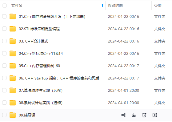
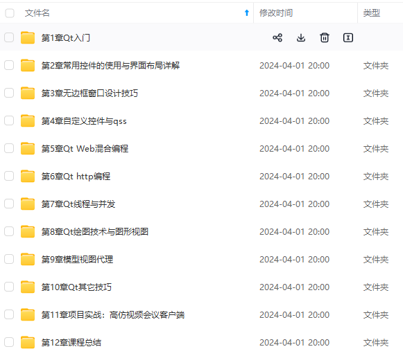
网上学习资料一大堆,但如果学到的知识不成体系,遇到问题时只是浅尝辄止,不再深入研究,那么很难做到真正的技术提升。
一个人可以走的很快,但一群人才能走的更远!不论你是正从事IT行业的老鸟或是对IT行业感兴趣的新人,都欢迎加入我们的的圈子(技术交流、学习资源、职场吐槽、大厂内推、面试辅导),让我们一起学习成长!
(address, DEC);
Serial.print(“!\nExpected:”);
for (j = 0; j < chunkSize; j++) {
Serial.print(" 0x");
if (progBuffer[j] < 16) Serial.print(“0”);
Serial.print(progBuffer[j], HEX);
}
Serial.print(“\nReceived:”);
for (uint8_t j = 0; j < chunkSize; j++) {
Serial.print(" 0x");
if (verifyBuffer[i + j] < 16) Serial.print(“0”);
Serial.print(verifyBuffer[i + j], HEX);
}
Serial.print(“\n”);*/
return false;
}
}
}
// increase byte index by [chunkSize]
i += chunkSize;

// uint8_t automatically wraps to 0 at 256
address += chunkSize;

// if we aren't done, update bank (if necessary) and address
if (i < dataSize)
{
  if (address == 0)
    bank++;
  mpu6500SetMemoryBank(bank, true, true);
  mpu6500SetMemoryStartAddress(address);
}
}
return true;
}
bool mpu6500WriteProgMemoryBlock(const uint8_t *data, uint16_t dataSize, uint8_t bank,
uint8_t address, bool verify)
{
return mpu6500WriteMemoryBlock(data, dataSize, bank, address, verify);
}
#define MPU6500_DMP_CONFIG_BLOCK_SIZE 6
bool mpu6500WriteDMPConfigurationSet(const uint8_t *data, uint16_t dataSize)
{
uint8_t *progBuffer, success, special;
uint16_t i;
// config set data is a long string of blocks with the following structure:
// [bank] [offset] [length] [byte[0], byte[1], …, byte[length]]
uint8_t bank=0;
uint8_t offset=0;
uint8_t length=0;
for (i = 0; i < dataSize;)
{
bank = data[i++];
offset = data[i++];
length = data[i++];
[外链图片转存中…(img-f7LNoXK7-1715616671420)]
[外链图片转存中…(img-ls5gjFvV-1715616671420)]
网上学习资料一大堆,但如果学到的知识不成体系,遇到问题时只是浅尝辄止,不再深入研究,那么很难做到真正的技术提升。
一个人可以走的很快,但一群人才能走的更远!不论你是正从事IT行业的老鸟或是对IT行业感兴趣的新人,都欢迎加入我们的的圈子(技术交流、学习资源、职场吐槽、大厂内推、面试辅导),让我们一起学习成长!


 1447
1447

 被折叠的 条评论
为什么被折叠?
被折叠的 条评论
为什么被折叠?
 到【灌水乐园】发言


