


指令集手册下载:Intel® 64 and IA-32 Architectures Software Developer Manuals
4800多页的PDF,分4卷,本文基于 April 2022的文档
Volume 1 - 7.1 PROGRAMMING ENVIRONMENT FOR GP INSTRUCTIONS、7.2 PROGRAMMING ENVIRONMENT FOR GP INSTRUCTIONS IN 64-BIT MODE
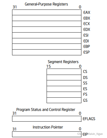
1、通用寄存器
32位
General-purpose registers — Eight 32-bit general-purpose registers (see Section 3.4.1,“General-Purpose Registers”) are used in non-64-bit modes to address operands in memory. These registers are referenced by the names EAX, EBX, ECX, EDX, EBP, ESI EDI, and ESP
Volume 1 - 3.4.1 General-purpose registers
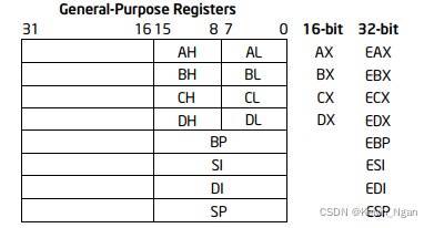
64位
General-purpose registers — In 64-bit mode, sixteen general-purpose registers available. These include the eight GPRs described in Section 7.1 and eight new GPRs (R8D-R15D). R8D-R15D are available by using a REX prefix. All sixteen GPRs can be promoted to 64 bits. The 64-bit registers are referenced as RAX, RBX, RCX, RDX, RBP, RSI, RDI, RSP and R8-R15 (see Section 3.4.1.1, “General-Purpose Registers in 64-Bit Mode”). Promotion to 64-bit operand requires REX prefix encodings.
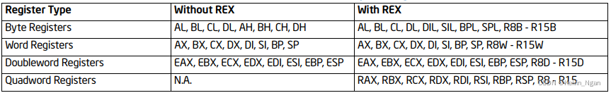
除了从32位的EXX寄存器扩展到64位的RXX寄存器,还增加了R8-R15一共8个寄存器,支持 byte(R8B-R15B), word(R8W-R15W), dword(R8D-R15D), and qword(R8-R15)
2、段寄存器
32位
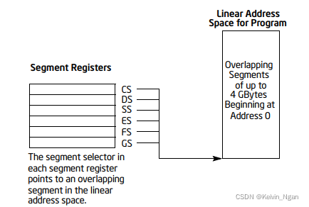
Segment registers — The six 16-bit segment registers contain segment pointers for use in accessing memory (see Section 3.4.2, “Segment Registers”). These registers are referenced by the names CS, DS, SS, ES, FS, and GS.
Volume 1 - 3.4.2 Segment registers

64位
In 64-bit mode: CS, DS, ES, SS are treated as if each segment base is 0, regardless of the value of the associated segment descriptor base. This creates a flat address space for code, data, and stack. FS and GS are exceptions. Both segment registers may be used as additional base registers in linear address calculations (in the addressing of local data and certain operating system data structures). Even though segmentation is generally disabled, segment register loads may cause the processor to perform segment access assists. During these activities, enabled processors will still perform most of the legacy checks on loaded values (even if the checks are not applicable in 64-bit mode). Such checks are needed because a segment register loaded in 64-bit mode may be used by an application running in compatibility mode. Limit checks for CS, DS, ES, SS, FS, and GS are disabled in 64-bit mode.
3、标志寄存器
32位
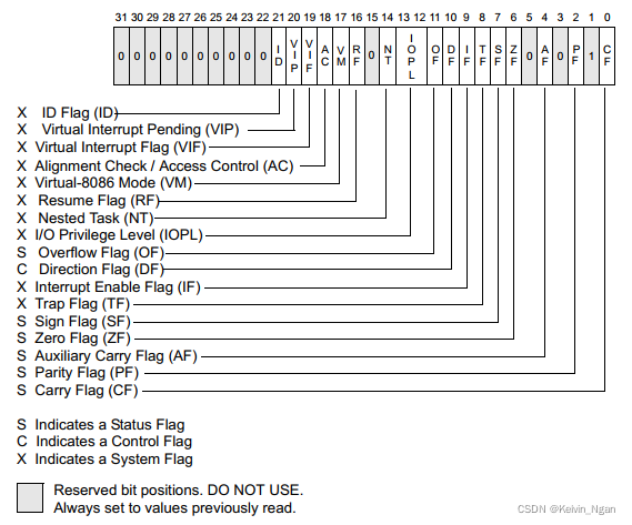
EFLAGS register — This 32-bit register (see Section 3.4.3, “EFLAGS Register”) is used to provide status and control for basic arithmetic, compare, and system operations.
Volume 1 - 3.4.3 EFLAGS registers
64位
Flags and Status register — When the processor is running in 64-bit mode, EFLAGS becomes the 64-bit RFLAGS register (see Section 3.4.3, “EFLAGS Register”).
In 64-bit mode, EFLAGS is extended to 64 bits and called RFLAGS. The upper 32 bits of RFLAGS register is reserved. The lower 32 bits of RFLAGS is the same as EFLAGS.
高32位作为保留位
4、指令指针寄存器
32位
Volume 1 - 3.5 Instruction Pointer
The instruction pointer (EIP) register contains the offset in the current code segment for the next instruction to be executed. It is advanced from one instruction boundary to the next in straight-line code or it is moved ahead or backwards by a number of instructions when executing JMP, Jcc, CALL, RET, and IRET instructions.
The EIP register cannot be accessed directly by software; it is controlled implicitly by control-transfer instructions (such as JMP, Jcc, CALL, and RET), interrupts, and exceptions. The only way to read the EIP register is to execute a CALL instruction and then read the value of the return instruction pointer from the procedure stack. The EIP register can be loaded indirectly by modifying the value of a return instruction pointer on the procedure stack and executing a return instruction (RET or IRET). See Section 6.2.4.2, “Return Instruction Pointer.”
All IA-32 processors prefetch instructions. Because of instruction prefetching, an instruction address read from the bus during an instruction load does not match the value in the EIP register. Even though different processor generations use different prefetching mechanisms, the function of the EIP register to direct program flow remains fully compatible with all software written to run on IA-32 processors.
64位
In 64-bit mode, the RIP register becomes the instruction pointer. This register holds the 64-bit offset of the next instruction to be executed. 64-bit mode also supports a technique called RIP-relative addressing. Using this technique, the effective address is determined by adding a displacement to the RIP of the next instruction
5、浮点寄存器
x87 Floating-Point Unit (FPU)
Volume 1 - 8.1.2 x87 FPU Data Registers
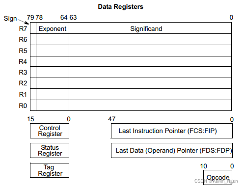
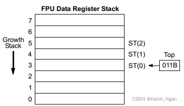
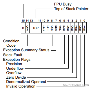
The x87 FPU instructions treat the eight x87 FPU data registers as a register stack (见下图). All addressing of the data registers is relative to the register on the top of the stack. The register number of the current top-of-stack register is stored in the TOP (stack TOP) field in the x87 FPU status word. Load operations decrement TOP by one and load a value into the new top-of-stack register, and store operations store the value from the current TOP register in memory and then increment TOP by one. (For the x87 FPU, a load operation is equivalent to a push and a store operation is equivalent to a pop.) Note that load and store operations are also available that do not push and pop the stack.
ST(0)-S(7)
FPU与MMX指令共享标志寄存器
the x87 FPU and Intel MMX technology share state because the MMX registers are aliased to the x87 FPU data registers. Therefore, when writing code that uses x87 FPU and MMX instructions, the programmer must explicitly manage the x87 FPU and MMX state
FPU标志寄存器
6、MMX寄存器.
Volume 1 - 9.2.2 MMX Registers
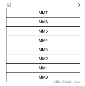
MMX registers — These eight registers (see Figure 9-1) are used to perform operations on 64-bit packed integer data. They are named MM0 through MM7.
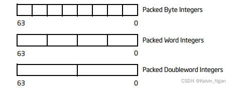
数据打包格式
64-bit packed byte integers — eight packed bytes (8 BYTE)
64-bit packed word integers — four packed words (4 WORD)
64-bit packed doubleword integers — two packed doublewords (2 DWORD)
Although MMX registers are defined in the IA-32 architecture as separate registers, they are aliased to the registers in the FPU data register stack (R0 through R7).
与FPU共用寄存器
7、XMM寄存器
Volume 1 - 10.2.2 XMM Registers
32位
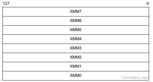
Eight 128-bit XMM data registers were introduced into the IA-32 architecture with SSE extensions (见下图). These registers can be accessed directly using the names XMM0 to XMM7; and they can be accessed independently from the x87 FPU and MMX registers and the general-purpose registers (that is, they are not aliased to any other of the processor’s registers).
64位
In 64-bit mode, eight additional XMM registers are accessible. Registers XMM8-XMM15
再增加8个寄存器
数据打包格式
SSE:
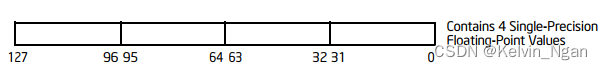
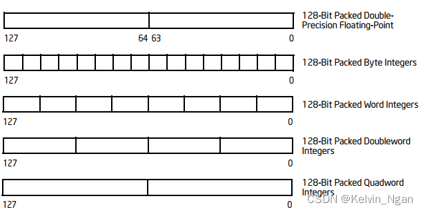
128-Bit Packed Single-Precision Floating-Point (4个单精度浮点数)
SSE2:
Packed double-precision floating-point(2个双精度浮点数)
128-bit packed integers(16 BYTE、8 WORD、4 DWORD、2QWORD)
SSE3、SSSE3、SSE4相比SSE、SSE2没有增加新的格式。同理,对于后面的256 AVX和512 AVX都是扩展了广播的宽度,并没有引入新的数据类型。
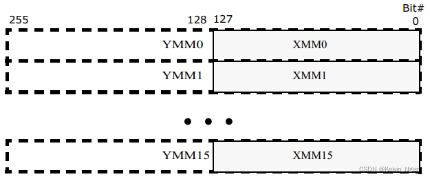
8、YMM寄存器
Volume 1 - 14.1.1 256-Bit Wide SIMD Register Support
Intel AVX introduces support for 256-bit wide SIMD registers (YMM0-YMM7 in operating modes that are 32-bit or less, YMM0-YMM15 in 64-bit mode). The lower 128-bits of the YMM registers are aliased to the respective 128-bit XMM registers. Legacy SSE instructions (i.e., SIMD instructions operating on XMM state but not using the VEX prefix, also referred to non-VEX encoded SIMD instructions) will not access the upper bits beyond bit 128 of the YMM registers. AVX instructions with a VEX prefix and vector length of 128-bits zeroes the upper bits (above bit 128) of the YMM
register.
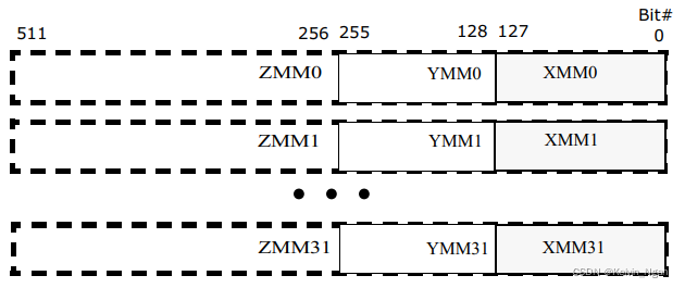
9、ZMM寄存器
Volume 1 - 15.1.1 512-Bit Wide SIMD Register Support
Intel AVX-512 instructions support 512-bit wide SIMD registers (ZMM0-ZMM31). The lower 256-bits of the ZMM registers are aliased to the respective 256-bit YMM registers and the lower 128-bit are aliased to the respective 128-bit XMM registers.


 4861
4861


 被折叠的 条评论
为什么被折叠?
被折叠的 条评论
为什么被折叠?
 到【灌水乐园】发言


