


最近要调试的一块电路板使用了10Pin 2.54mm间距的接插件,买来的ulink2只提供了20Pin的数据线,于是只能自己做连接线了。拆开ulink2外壳,激动的发现有10pin的过孔,可仔细一看上面写着"51-2Pin"字样,拿万用表量了下导通,果然不是ARM用的。看来只能从20Pin的ARM管脚上飞线出来了,看了下手册,JTAG/SWD 20Pin的管脚定义比10Pin的多了十个冗余的NC/GND管脚,也就是说只要照着定义改就成了。搞硬件的同事都忙,于是本码农只能自己拿起烙铁了。于是有了下图的大作 话说实验室的工具和线材还挺齐全的。

ULINK2 provides five JTAG connectors. They support various cable types, which are used for debugging different targets. The connectors provided are:
- A narrow (2.00mm/0.079") pin spacing) 20-pin connector for ARM targets,
- A standard (2.54mm/0.1") 20-pin connector for ARM targets,
- A 16-pin connector for Infineon OCDS (JTAG) targets,
- A 14-pin connector for STMicroelectronics µPSD targets,
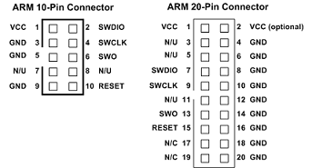
- and a 10-pin connector for ARM targets (Mfgr: Don Connex P/N: C42 or Samtec P/N: SHF-105-01-L-D-TH). The Samtec part is available with different options for plating, tail, shroud, and lead style.
A cable for each connector is shipped with the ULINK2 Standard Product. If you must change cables, then make sure to line up the marker stripe on the cable with pin 1 of the connector. Pin 1 is labeled on the board.

ULINK2 Adapter Connectors (cover off)
ULINK2 supports both JTAG and Serial Wire Mode interfaces. Refer to the appropriate pinout diagram for the ULINK2 adapter connectors to make sure they match your target hardware.
JTAG Interface

| Signal | Connects to... |
|---|---|
| TMS | Test Mode State pin — Use 100K Ohm pull-up resistor to VCC. |
| TDO | Test Data Out pin. |
| RTCK | JTAG Return Test ClocK. (see Note below) |
| TDI | Test Data In pin — Use 100K Ohm pull-up resistor to VCC. |
| TRST | Test ReSeT/ pin — Use 100K Ohm pull-up resistor to VCC. TRST is optional and not available on some devices. You may leave it unconnected. |
| TCLK | Test CLocK pin — Use 100K Ohm pull-down resistor to GND. |
| VCC | Positive Supply Voltage — Power supply for JTAG interface drivers. |
| GND | Digital ground. |
| RESET | RSTIN/ pin — Connect this pin to the (active low) reset input of the target CPU. |
| CPUCLK | CPU clock (according IEEE Standard 1149.1). |
| OCDSE | Enable/Disable OCDS interface (Infineon-specific). |
| TRAP | Trap condition (Infineon-specific). |
| BRKIN | Hardware break in (Infineon-specific). |
| BRKOUT | Hardware break out (Infineon-specific). |
| /JEN | JTAG Enable (STMicroelectronics specific). |
| TSTAT | JTAG ISP Status (STMicroelectronics specific) (optional). |
| /RST | Chip reset (STMicroelectronics specific). |
| /TERR | JTAG ISP Error (STMicroelectronics specific) (optional). |
Serial Wire Mode Interface
The Serial Wire (SW) mode is a different operating mode for the JTAG port where only two pins, TCLK and TMS, are used for the communication. A third pin can be use optionally to trace data. JTAG pins and SW pins are shared.
- TCLK is SWCLK (Serial Wire Clock)
- TMS is SWDIO (Serial Wire debug Data Input/Output)
- TDO is SWO (Serial Wire trace Output)
| Signal | Connects to... |
|---|---|
| SWDIO | Data I/O pin. Use 100K Ohm pull-up resistor to VCC. |
| SWO | Optional trace output pin. |
| SWCLK | Clock pin. Use 100K Ohm pull-down resistor to GND. |
| VCC | Positive Supply Voltage — Power supply for JTAG interface drivers. |
| GND | Digital ground. |
| RESET | RSTIN/ pin — Connect this pin to the (active low) reset input of the target CPU. |
Additional ARM 10-pin cables with connectors are available directly from Samtec:
- 6" Cable (Samtec P/N: FFSD-05-D-06.00-01-N)
- 12" Cable (Samtec P/N: FFSD-05-D-12.00-01-N)
 Note
Note
- ULINK2 is powered through the USB connection.
- ULINK2 operates at 3.3V. All JTAG pins are 5V tolerant.
- Usually, devices do not include pull-up or pull-down resistors on JTAG nor SW pins. Resistors should be added externally onto the board. However, do not add resistors when the device includes them already.
- Some NXP LPC2000 Devices have special pins (RTCK, DBGSEL) that enable the JTAG interface. For example, on the NXP LPC2129 the signal RTCK must be driven low during RESET to enable the JTAG interface. You may want to add jumpers to your hardware to accomplish this.


 2万+
2万+

 被折叠的 条评论
为什么被折叠?
被折叠的 条评论
为什么被折叠?
 到【灌水乐园】发言


