


电源(power supply)
原理图(schematic)
MY-I.MX6系列核心板,只需要一个5V电源(持续供电电流不低于2A,峰值2.5A-3A)输入即可。详见下图。
MY-I.MX6 series of core board only needs 5V power source(constant current is not small than 2A,peak value 2.5A-3A)as an input。details as below。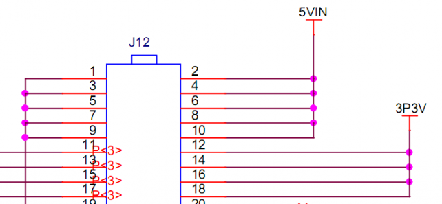
如果是直接的5V输入,5V的电源一定要做过压保护,过压保护电路参考如下。
IF it is a direct 5V input,5V power source need a over voltage protection,the protection circuit can be designed with following reference。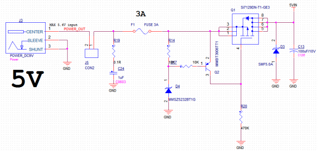
如果是高电压输入通过DCDC转换成5V,核心板会输出一个3P3V的电源,此电源的电流不超过500mA。如果底板上面3.3V的电流非常小,可以直接采用此3P3V作为底板的供电电源,如果用3P3V作为底板供电电源,请在3P3V电源上串上500mA的保险丝。
if it is high voltage input to be converted to 5V through DCDC principle,the core board will output 3P3V power source with a maximum current 500mA of which can be used as power supply for base board if current with 3.3V on the base board is too small,in this case,please put in serial a fuse for this 3P3V power source 。
由于底板上面的3.3V电压通常会超过500mA,一般用户会单独通过DCDC或者LDO产生3.3V。
since current with 3.3V on the base board is usually over 500mA,normally users will generate a another 3.3V through DCDC or LDO。
注意:底板的3.3V的电源,一定要通过核心板的3P3V来做使能控制,而不能够直接由底板上面的其他电源产生。如果底板上面还有其他电源,也必须有3P3V来做使能控制。此点是由于I.MX6芯片决定的。
note:enable control must be done for 3.3V on base board by 3P3V on core board instead of being conducted by other power sources on the base board.if there are other power sources on base board,their enable controls must be conducted by 3P3V as well,this is up to the nature of I.MX6 chip。
参考电路如下:
reference circuit as below: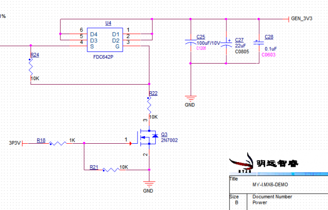
核心板5V电源输入处要放置大的储能电容,确保CPU在瞬间增加负载的时候不至于断电。如果有过孔,确保过孔的电流至少能够通过3A的峰值电流,可以多打一些过孔增加电流。
capacitor with big capacity should be placed near 5V input on core board, to ensure contituous power supply even when sudden extra load is added for CPU。if there is via hole,need to make sure via hole can go through 3A peak current,more via holes can be built to increase current。
串口设计(serial port design)
原理(principle)
串口设计上面,经常会碰到的问题是RXD跟TXD的方向接反。参考原理图中的网标表示如下
for serial port design,common questions arising are inversion between RXD and TXD。network standard in the schematic as below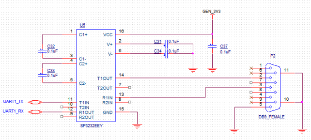
TXD——CPU输出
TXD——CPU output
RXD——CPU输入
RXD——CPU input
PCB
 最低0.47元/天 解锁文章


 490
490


 被折叠的 条评论
为什么被折叠?
被折叠的 条评论
为什么被折叠?
 到【灌水乐园】发言


