


IEEE ELECTRON DEVICE LETTERS, VOL, EDL-7, NO. 4, APRIL 1986
电气与电子工程师协会电子设备投稿栏,第四卷,电子器件7,1986年4月
A Vertical Kelvin Test Structure for Measuring the True Specific Contact Resistivity
一个测量真实的特定的接触电阻率的垂直温度测试结构
TAN FU LEI, MEMBER, IEEE, LEN-YI LEU, AND CHUNG LEN LEE
谭弗雷,成员,IEEE,
Abstract-A vertical kelvin test structure, which can be used to measure the true specific contact resistivity of a metallization system, is proposed and studied. For this test structure, the driving current flows"vertically," thus the sheet resistance and current crowding effects are eliminated and measurement on the ture specific contact resistivity becomes possible. Experimental works show that this test structure gives a more linear relation between resistance and contact area than the conventional six-terminal test structure.
摘要-垂直温度测试结构能够被用来测量真实的特定的金属化系统的接触电阻率,垂直温度测试结构被计划和学习。对于这个测试结构来说,驱动电流垂直地流过,从而片状的阻力和电流催逼效应被消除和在真实的特定的可接触电阻变得可能。实验性的工作展示了在电阻和接触面之间这个测试结构比传统的6-终端测试结构给出了更多的线性关系。
In this letter, a "vertical" kelvin test structure to measure the "true" specific contact resistivity is presented. For this test structure, the driving current flows "vertically" from the metal contact pad toward the contacted substrate. This eliminates the current crowding effects which are inherent in the horizontal type of test structures, and makes the determination of the "true" specific contact resistivity possible. This test structure can be incorporated with the six-terminal test structure [4] to compare the measured results.
在这个栏目里,测量“真实的”特定的接触电阻率的“垂直的”温度测试结构被推出。对于这个测试结构,驱动电流垂直地从金属制的接触衬垫流到接触基片。消除在这个测试结构的卧式中的电流聚集效应,造就了真实的特定的接触电阻可能性。这个测试结构能够和6-终端测试结构[4]合并来比较测量结果。
II. TEST STUCTURE
The cross section of the test structure is shown in Fig. 1(a) along with its top view in Fig. 1(b). The driving current I is forced from pad 1 toward the substrate and the voltage V is sensed between pads 2 and 3 along the implanted bar. The vertical current flow is restricted by an isolation p-n junction. For this structure, it can be seen that the current flows vertically and only through the contact window, hence the current distribution in the contact resion is uniform provided that the contact region is metallurgically uniform. The contact resistance Rc is thus directly measured with the value of V/I, where Ac is the contact area through which the current passes. No lateral current crowding effect, which is mentioned in [6] and [7], is expected. Also, the sheet resistance effect on determining the value of pc become minimum for this test structure since it is not involved at all in determining pc.
2. 测试结构
这个测试结构的横截面和它的顶视图图1(b)被展示在图1(a)。驱动电流I强迫衬垫1趋向基片,电压V被产生在沿着嵌入阀的衬垫2和3之间。垂直电流被一个绝缘PN结限制。对于这个测试结构,它能被看到电流仅仅通过接触窗口垂直地流过,因此如果这个接触区是金属制统一的在接触区的电流分配是统一的。接触电阻Rc可以使用V/I的值直接测量,Ac是电流通过的接触面。没有侧面电流聚集效应,侧面电流聚集效应将在第六和第七部分提及。同样的,虽然表面电阻不能对pc产生根本影响,对于这个测试结构来说表面电阻对pc流变成最小值有一定影响。
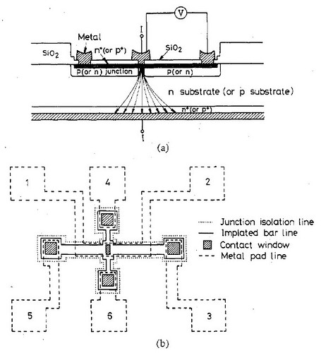
Fig. 1. (a) The cross-sectional view of the proposed vertical Kelvin test
structure for measuring the true specific contact resistivity. (b) The top view
of the structure. In the figure, the horizontal structure for the six-terminal
measurement is also incorporated.
图1(a)测量真实特定接触电阻率的垂直温度测试结构的横截面图
图1(b)测量真实特定接触电阻率的垂直温度测试结构的顶视图。在这个图里,6-终端测量的水平结构也被加入进来
Manuscript received September 18, 1985; revised December 2, 1985. This work was supported by Electronic Research and Service Organization (ERSO), ITRI of Taiwan, Republic of China.
The authors are with the Institute of Electronics, National Chiao Tung University, Hsin Chu, Taiwan, Republic of China.
IEEE Log Nmber 8608010.
手稿在1985年9月18日接收,1985年12月2日校订。这项工作被电子开发和服务组织(ERSO),台湾的ITRI,中华人民共和国所支持。
作者包括国民交通大学电子学院,Hisn Chu,台湾,中华人民共和国
国际电子与电气工程师协会历史记录数字 8608010.
In Fig.1, the six-terminal structure [4] is also incorporated and this has two merits. First, the voltage V can also be sensed between pad pairs 2-4, 2-5, and 2-6. The obtained values can be averaged with that of the pad pair 2-3 to reduce the error introduced by the misalignment between the isolation junction window and the contact window. Second, six-terminal measurement can be performed and the result can be compared with that obtained from the vertical structure.
在图1中,6-终端结构(图标4)也被合并进来,这样做有两个优点。第一,电压V也能在衬垫对2-4、2-5、2-6之间产生。所获得的值能够被平均防止因为孤立界面和接触界面之间的未对准引入的错误。第二,6-终端测量能够被执行,结果能够与来自于垂直结构的值做比较。
III. EXPERIMENTS AND RESULTS
Test structures of Fig.1 have been fabricated to compare the results obtained by the vertical structure measrement and the six-terminal measurement, respectively. Different contact systems of either A1(1-percent Si)/Si or A1(1-
((0741-3106/86/0400-0259$01.00 © 1986 IEEE
percent Si)/TiSi2/Si were formed on n-type substrates of the resistivity of 3~5 Ω·cm. Contact regions of various dimensions (5X5 µm, 5X10 µm, 10X10 µm, 10X15 µm, 10X20 µm, 15X15 µm, 15X20 µm, 20X20 µm) were used. The alignment tolerance of the contact was 10 µm. The n+ implanted bars and the p isolation junctions were formed by ion implantation and the junctions were kept as shallow as possible. The depths of n+ junctions were 0.33-0.5 µm for 2 x 10(15)/cm2 to 6 x10(15)/cm2 ion doses of As+ and the junction depths of p isolations were 0.7 pm for 2 x 10(13)/cm(2) ion dose of BF2+. The backsides of wafer were n+ diffused and A1 metallized. For each wafer, at least 200 test patterns were measured.
3. 实验和结果
图1的测试结构已经被制造来比较通过垂直结构测量和6-终端测量的结果。分别的,不同的接触系统1%硅/硅或者1%硅/Ti硅/硅在电阻率为3~5欧姆/厘米的N型基片上加工成型。各种各样规模(5X5 纳米,5X10 纳米, 10X10纳米, 10X15纳米, 10X20 纳米, 10X20 纳米, 15X15 纳米, 15X20 纳米, 20X20 纳米)的接触面被使用。接触的定位公差是10纳米。n
 最低0.47元/天 解锁文章


 被折叠的 条评论
为什么被折叠?
被折叠的 条评论
为什么被折叠?
 到【灌水乐园】发言


