


 本文探讨了人工智能芯片领域的最新趋势,重点分析了GPU、TPU和FPGA在AI计算中的应用及初创公司的发展。通过翻译自Medium的文章,读者可以了解到这些芯片在大数据处理和物联网中的关键作用。
ai芯片fpga
Major tech companies invest billions in AI chip development. Even Microsoft and Facebook are onboard with Intel FPGA in accelerating their hardware infrastructures. There are a handful of startups that are already unicorns but there are sad stories like Wave Computing that filed for bankruptcy after raising 187 million in 3 years. In this series, we will cover about 30 companies. We will focus on the technology landscape with an emphasis on identifying future advancements and trends.
大型科技公司在AI芯片开发上投资了数十亿美元。 甚至Microsoft和Facebook也加入了Intel FPGA来加速其硬件基础架构。 有少数已经成为独角兽的初创公司,但有像Wave Computing这样的悲伤故事,它们在三年内筹集了1.87亿美元后申请破产。 在本系列中,我们将涵盖约30家公司。 我们将专注于技术领域,重点是确定未来的进步和趋势。
This series will be split into 3 parts. The first article looks at the development trends for GPU, TPU, FPGA, and Startups. The first three categories represent the largest market share in AI acceleration. We will focus on what vendors have been improving. Hopefully, it tells us where they may go next. In the second half of this article, we look at novel approaches popular by startups. In particular, many of them move away from instruction flow designs to dataflow designs. This is a major paradigm shift that can change the AI chip direction completely. So let’s spend some time studying it.
该系列将分为3部分。 第一篇文章介绍了GPU,TPU,FPGA和Startups的发展趋势。 前三个类别代表了AI加速的最大市场份额。 我们将重点关注供应商正在改进的方面。 希望它告诉我们他们下一步可能去哪里。 在本文的下半部分,我们将介绍初创公司流行的新颖方法。 特别是,它们中的许多都从指令流设计转移到了数据流设计。 这是一个重大的范式转换,可以完全改变AI芯片的方向。 因此,让我们花一些时间研究它。
英伟达GPU (Nvidia GPU)
GV100 (Volta architecture) is released in late 2017 while GA100 (Ampere architecture) is released in 2020.
GV100(Volta架构)于2017年末发布,而GA100(Ampere架构)于2020年发布。
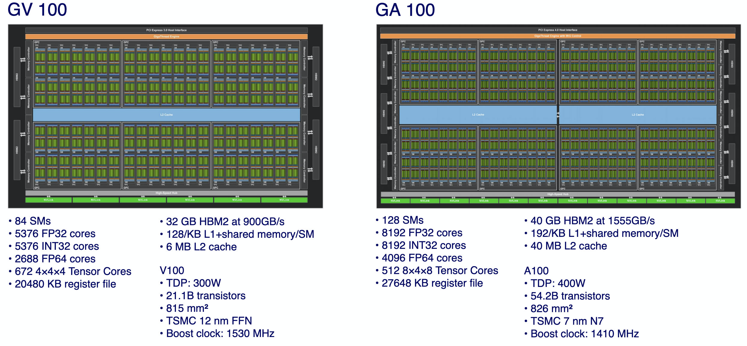
GA 100 GPU uses the TSMC 7 nm fabrication instead of the 12 nm process in GV 100. While their die sizes are about the same, the number of Streaming Multiprocessors (SMs) in GA100 is increased by 50% to 128 and the number of FP32 cores is increased from 5376 to 8192. The new Gen3 Tensor Cores perform 8×4 by 4×8 matrix multiplication instead of 4×4 by 4×4.(Details)
GA 100 GPU使用台积电7纳米制造Craft.io代替了GV 100中的12纳米Craft.io。虽然它们的芯片尺寸大致相同,但GA100中的流式多处理器(SM)的数量增加了50%,达到128个,FP32的数量增加了核心从5376增加到8192。新的Gen3张量核心执行4×8矩阵乘法的8×4而不是4×4×4×4的矩阵。( 详细信息 )
So far, these trends are pretty expected in many AI chips — more cores with better matrix multiplication units targeted for deep learning (DL). But there are some noticeable design enhancements.
到目前为止,这些趋势在许多AI芯片中都是可预见的-更多的内核具有针对深度学习(DL)的更好的矩阵乘法单元。 但是,在设计上有一些明显的增强。
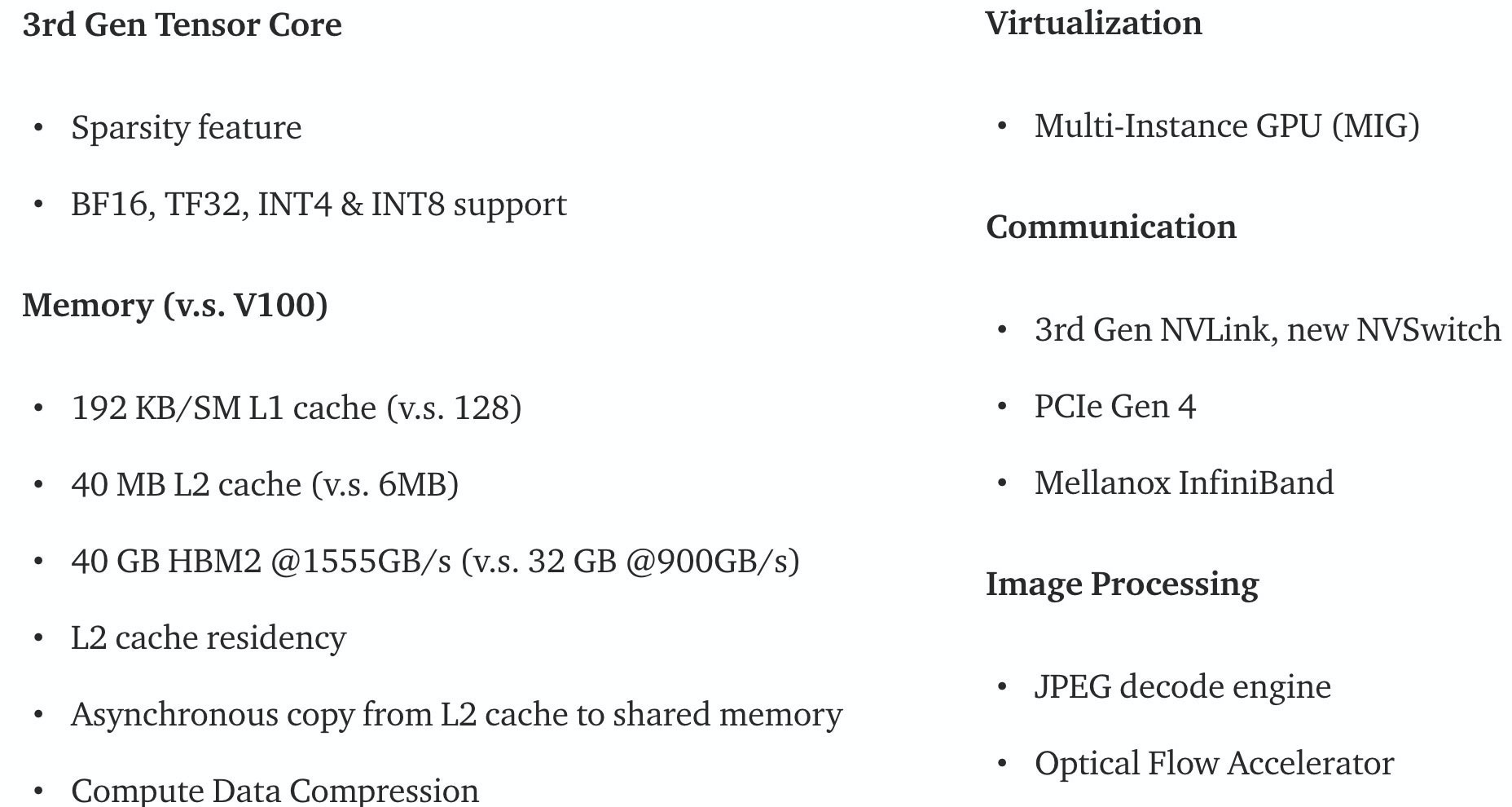
First, it addresses potential memory bottlenecks. The L2 level cache increases un-proportionally from 6MB to 40MB. The L1 cache per SM increases by 50%. In addition, developers have more control over what data to be cached on L2 and the flexibility of by-passing L1 in copying data directly to the SM shared memory.
首先,它解决了潜在的内存瓶颈。 L2级别的缓存从6MB不成比例地增加到40MB。 每个SM的L1缓存增加了50%。 此外,开发人员可以更好地控制要在L2上缓存哪些数据,以及在将数据直接复制到SM共享内存时绕过L1的灵活性。
Second, DNNs (deep neural networks) weight sparsity is heavily exploited. After data compression, the data volume transmitted between the off-chip memories and the on-chip cache decrease significantly by 2x to 4x. With this sparsity, the Tensor Core is redesigned for even faster operations.
其次, DNN (深度神经网络)权重稀疏性被大量利用。 数据压缩后,在片外存储器和片上高速缓存之间传输的数据量显着减少了2倍至4倍。 由于这种稀疏性,Tensor Core被重新设计以实现更快的操作。
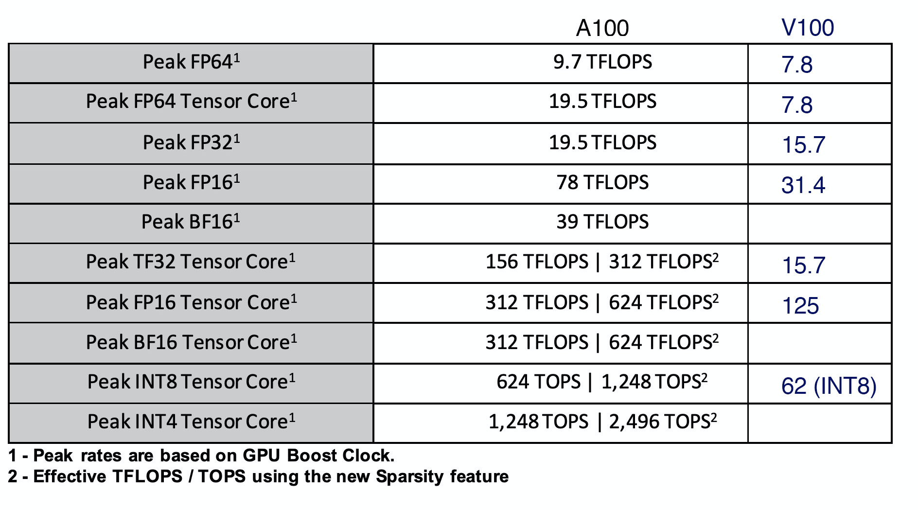
Third, more data type (BF16, INT4, TF32) is supported. In DL, the general trend is 16-bit matrix arithmetic with the value range equals FP32 for training and hopefully even 8 bit for inference. As shown below, some improvements are in one order of magnitude for lower precision arithmetics.
第三,支持更多数据类型(BF16,INT4,TF32)。 在DL中,一般趋势是16位矩阵算术,其值范围等于FP32进行训练,希望甚至达到8位进行推理。 如下所示,对于较低精度的算术,一些改进在一个数量级上。
Fourth, faster inter-GPU communications to handle model training that cannot fit into one GPU.
第四,更快的GPU间通信以处理无法适合一个GPU的模型训练。
Fifth, new features are created, like video encoding/decoding, for end-to-end solutions.
第五,为端到端解决方案创建了新功能,例如视频编码/解码。
These trends are very important as we look at many AI companies. These are the same problems that chip designers are solving but just not necessarily the same solution. Sparsity and memory bandwidth will remain important for future development. But besides hardware support in weight sparsity, data sparsity, and weight updates will be heavily studied (more on this in part 2).
当我们关注许多AI公司时,这些趋势非常重要 。 这些是芯片设计人员正在解决的相同问题,但不一定是相同的解决方案。 稀疏性和内存带宽对于将来的开发将仍然很重要。 但是,除了对重量稀疏性的硬件支持之外,还将对数据稀疏性和重量更新进行大量研究(第2部分将对此进行详细介绍)。
In addition, NVidia is the most mature AI chips provider. As dealing with real customer needs, GPU virtualization (MIG feature turns a single GPU into multiple virtual GPUs) is added for better utilization in cloud-based inferencing.
此外,NVidia是最成熟的AI芯片提供商。 在满足实际客户需求时,添加了GPU虚拟化(MIG功能将单个GPU变成多个虚拟GPU),以更好地利用基于云的推理。
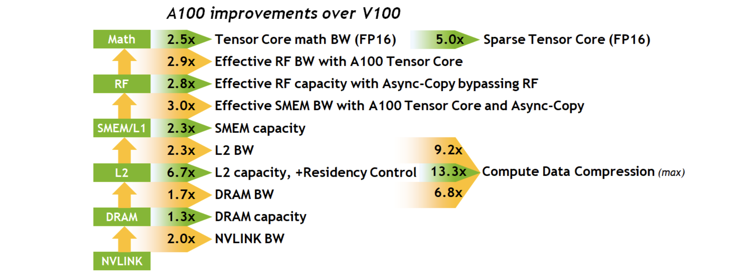
For reference, these are the magnitude of performance improvements made in A100 GPU over V100 for the specific enhancements.
作为参考,这些是A100 GPU在V100上针对特定增强所做的性能改进幅度。
Google TPU (Google TPU)
A general GPU provides the programmability that many projects may consider as “fat”. So it comes back to the question of whether this hurts or not. For Google, many servers are allocated to solving specific problems. Small improvements can save millions. Specifically, GPU consumes more energy than ASIC (Application-specific integrated circuit) and has higher latency.
通用GPU提供了许多项目可能认为是“胖”的可编程性。 因此,这又回到了是否有伤害的问题。 对于Google,分配了许多服务器来解决特定问题。 小小的改进可以节省数百万美元。 具体而言,GPU比ASIC(专用集成电路)消耗更多的能量,并且具有更高的延迟。
Chip companies can design ASIC chips for maximum efficiency. But development costs are expensive and not adaptable to changes. Since the breakout success of AI in 2012, Google has gathered abundant experience in narrow down these design requirements. In fact, it concludes that Google TPU just needs high throughput for matrix multiplication, activation, normalization, and pooling.
芯片公司可以设计ASIC芯片以实现最高效率。 但是开发成本昂贵,并且无法适应变化。 自2012年AI取得突破性成功以来,Google在缩小这些设计要求方面积累了丰富的经验。 实际上,得出的结论是,Google TPU仅需要高吞吐量即可进行矩阵乘法,激活,归一化和池化。
TPU (details) takes away many control logic, in particular, dealing with instruction fetching and scheduling. It shifts this work to the CPU host. TPU simply acts as a coprocessor and provides vertical instructions.
TPU( 详细信息 )取消了许多控制逻辑,尤其是处理指令提取和调度的逻辑。 它将工作转移到CPU主机。 TPU只是充当协处理器并提供垂直指令。
This leads to a very important design trend in general.
通常,这导致非常重要的设计趋势。
Works, like instruction scheduling, optimization and resource assignments is shifted to the runtime library in CPU and the compiler.
指令调度,优化和资源分配等工作已转移到CPU和编译器中的运行时库中。
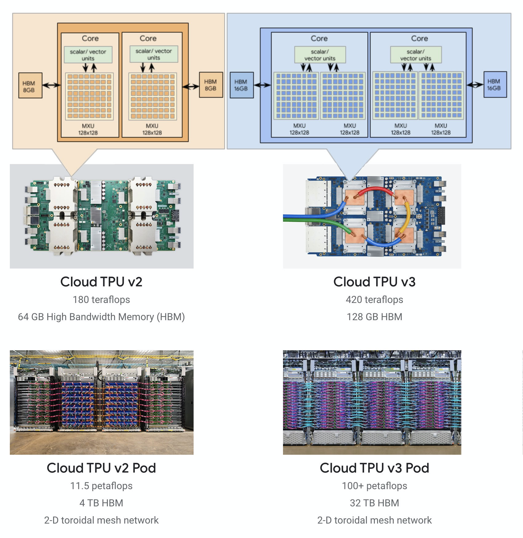
As shown in the diagram below, TPU v3 doubles the number of cores than v2, and TFLOPs is a little bit more than double. The coming TPU v4 will double in performance again (2.7x). The throughput of its matrix multiplication units has been more than double. Not much else is known yet but it will not be surprising if the number of cores is double or the matrix multiplication size has increased. But this has increased the memory bandwidth requirement significantly which is solved with unspecified advances in interconnect technology.
如下图所示,TPU v3的内核数量是v2的两倍,而TFLOP则是两倍多。 即将面世的TPU v4的性能将再次翻倍(2.7倍)。 它的矩阵乘法单元的吞吐量已增加了一倍以上。 到目前为止,还没有多少其他信息,但是如果核心数增加一倍或矩阵乘法大小增加,也就不足为奇了。 但这极大地增加了内存带宽需求,而互连技术的未指定进步解决了这一需求。
Google has the monetary resource, powers, and wills to build a vertical solution. Their own datacenters and cloud services already provide a mature market for TPUs. Keep things focus, keep it simple, and optimize what matters seem to be the key focus for TPU.
Google拥有金钱资源,能力和意愿来建立纵向解决方案。 他们自己的数据中心和云服务已经为TPU提供了成熟的市场。 保持重点,使其简单,并优化问题,这似乎是TPU的重点。
英特尔FPGA (Intel FPGA)
However, the rigidity of ASIC bothers companies like Facebook or Microsoft. For better flexibility in designs and options, they are looking into solutions like FPGA. The hardware design for GPU and TPU cannot be changed. But for decades, FPGA has allowed hardware designers for reconfigurable ASIC design that can be reprogrammed in ∼20ms.
但是,ASIC的僵化困扰着Facebook或Microsoft等公司。 为了使设计和选项具有更好的灵活性,他们正在研究诸如FPGA之类的解决方案。 GPU和TPU的硬件设计无法更改。 但是几十年来,FPGA允许硬件设计人员进行可重配置的ASIC设计,该设计可在约20ms内重新编程。
FPGA Overview (Optional)
FPGA概述(可选)
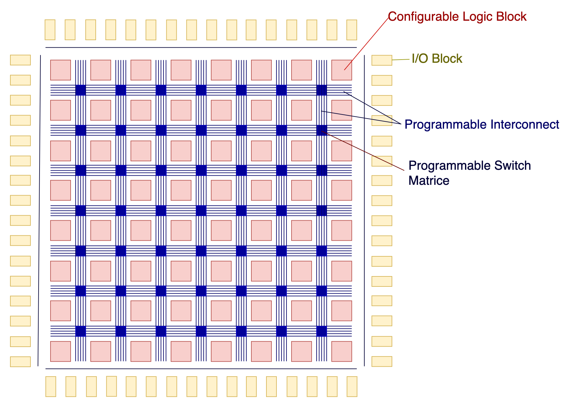
Software engineers are less familiar with FPGA. So let’s have a simple overview. FPGA contains an array of blocks for logic and arithmetic functions. FPGA has put many thoughts on its reconfigurability in creating custom functions in each block. In addition, these blocks can be connected through programmable interconnect to build custom features with specific concurrency, latency, I/O throughput, and power consumption.
软件工程师对FPGA不太熟悉。 因此,让我们进行简单的概述。 FPGA包含一系列用于逻辑和算术功能的模块。 FPGA在每个块中创建自定义函数时已经考虑了其可重新配置性。 此外,这些模块可以通过可编程互连进行连接,以构建具有特定并发性,延迟,I / O吞吐量和功耗的自定义功能。
FPGA also provides blocks, like those for local memory and IP blocks (a.k.a. reusable hardware cell design) for vertical solutions. Particularly, DSP blocks, optimizing vector and multiplications, have been repurposed for ML/DL acceleration.
FPGA还提供用于垂直解决方案的块,例如用于本地存储器的块和IP块(也称为可重用硬件单元设计)。 特别是,优化矢量和乘法的DSP块已重新用于ML / DL加速。

Intel FPGA
英特尔FPGA
Microsoft Project Brainwave uses Intel Stratix 10 FPGA to accelerates DNN inferencing in services like Bing’s intelligent search features and Azure. Other Intel FPGA product lines are offered, including Agilex (high-end) and Arria for different market segments.
Microsoft Project Brainwave使用Intel Stratix 10 FPGA来加速Bing的智能搜索功能和Azure等服务中的DNN推理。 提供了其他英特尔FPGA产品线,包括针对不同细分市场的Agilex(高端)和Arria。
Like GPU, FPGA is originally designed for different markets. FPGA offers fine-grain connectivity among blocks in building customized functions. But this is “fat” for AI chips in some context. The fine grain connectivity responsible for the interconnect increases the die size significantly. It also increases latency and power consumption. AI chips need coarse-grain connectivity with more complex blocks. To address these needs, specialized AI IP blocks are created. For example, Intel Stratix 10 NX FPGA is particularly designed with AI Tensor Blocks. These blocks contain dense arrays of lower-precision multipliers optimized for matrix and vector multiplications with INT4, INT8, Block FP12, or Block FP16 operations. In addition, these tensor blocks can be cascaded together to support large matrices.
像GPU一样,FPGA最初是为不同的市场设计的。 FPGA在构建定制功能时提供了各模块之间的细粒度连接。 但这在某些情况下对于AI芯片来说是“肥胖”。 负责互连的细颗粒连通性显着增加了芯片尺寸。 它还增加了延迟和功耗。 AI芯片需要具有更复杂块的粗粒度连接。 为了满足这些需求,创建了专门的AI IP块。 例如,英特尔Stratix 10 NX FPGA是专门为AI Tensor模块设计的。 这些块包含低精度乘法器的密集数组,这些数组针对使用INT4,INT8,Block FP12或Block FP16运算的矩阵和矢量乘法进行了优化。 此外,这些张量块可以级联在一起以支持大型矩阵。

DNN layers mapping
DNN图层映射
However, there is a huge gap between AI models and FPGA programming which speaks about clock and signals. In FPGA, designers use HDL (Hardware Description Language) to describe the hardware design which later compiled into bitstreams to reconfigure the chip. In AI, FPGA vendors heavily invest in bitstreams specialized in optimizing each DL models like ResNet, GoogleNet, etc…
但是,AI模型与FPGA编程之间存在巨大的差距,这涉及时钟和信号。 在FPGA中,设计人员使用HDL(硬件描述语言)来描述硬件设计,然后将其编译为比特流以重新配置芯片。 在AI中,FPGA供应商大量投资于专门优化每个DL模型(例如ResNet,GoogleNet等)的比特流。
In these bitstreams, DNN layers are mapped into a pipeline for processing, similar to TPU. In the example below, AlexNet layers are grouped into blocks containing the CNN layer, ReLU, normalization, and max pool. Each block will be executed in the pipeline with a stream buffer holding intermediate calculations.
在这些比特流中,类似于TPU,DNN层被映射到管道中进行处理。 在下面的示例中,AlexNet层被分组为包含CNN层,ReLU,规范化和最大池的块。 每个块都将在流水线中执行,并带有保存中间计算的流缓冲区。

These blocks are highly reconfigurable in runtime and bypassable.
这些块在运行时高度可重新配置并且可以绕过。

With the flexibility of designing your own hardware, it can implement algorithms, like Winograd Transform in accelerating the CNN convolution.
凭借设计自己的硬件的灵活性,它可以实现算法,例如Winograd Transform,以加速CNN卷积。

This architecture is realized by having an array of Convolution Processing Element (PE) connected to ReLU, Norm, and Max Pool module through a crossbar. To provide better flexibility that ASIC, custom blocks can be compiled and attached to the crossbar below for new DNN layer designs.
通过将卷积处理元素(PE)阵列通过交叉开关连接到ReLU,Norm和Max Pool模块,可以实现此体系结构。 为了提供比ASIC更好的灵活性,可以编译自定义块并将其附加到下面的交叉开关上,以进行新的DNN层设计。

Without starting from scratch, FPGA provides the flexibility of using vertical IP blocks and specialized bitstreams in customizing a new hardware design that aimed for ASIC-like performance.
从头开始,FPGA提供了使用垂直IP块和专用位流的灵活性,以定制旨在实现类似于ASIC性能的新硬件设计。
赛灵思ACAP (Xilinx ACAP)
Xilinx Versal is an Adaptive Compute Acceleration Platform (ACAP). ACAP is a heterogeneous compute platform that combines Scalar Engines, Adaptable Engines (a.k.a. configurable logic block CLB), and AI Engines. We can view this as the AI version for SoC (system on chip). All these engines are interconnected with the network-on-chip (NoC) in achieving multi-terabit communication.
Xilinx Versal是一个自适应计算加速平台(ACAP)。 ACAP是一个异构计算平台,结合了标量引擎,自适应引擎(也称为可配置逻辑块CLB)和AI引擎。 我们可以将其视为SoC(片上系统)的AI版本。 所有这些引擎都与片上网络(NoC)互连,以实现多太比特通信。

The AI Engines contains an array of VLIW/SIMD vector cores with tightly coupled local memory. Like FPGAs, it is highly configurable for specialized hardware design and it is targeted for DL inference.
AI引擎包含具有紧密耦合的本地内存的VLIW / SIMD矢量核阵列。 像FPGA一样,它可高度配置以用于专门的硬件设计,并且是DL推理的目标。

灵活性和泛化 (Flexibility and Generalization)
The flexibility in FPGA helps big software companies to accelerate a specific set of AI applications in their massive data center. Microsoft Brainwave project with Intel is one of them. The power consumption and latency are targeted to match ASIC designs. But the hardware reconfigurability is the key selling point without sticking into one design plan.
FPGA的灵活性可帮助大型软件公司在其大规模数据中心中加速一组特定的AI应用程序。 与英特尔合作的Microsoft Brainwave项目就是其中之一。 功耗和等待时间旨在匹配ASIC设计。 但是,硬件可重配置性是关键的卖点,而无需遵守一项设计计划。
This leads to one critical question for chip companies. Generalization acts against performance and power consumption. What market fit do you want your product to be? How much flexibility are you willing to provide at the cost of efficiency and performance? Is the chip targeted for inference, training, or both? Betting on the wrong spot will cost the future of the product if not the company.
这给芯片公司带来了一个关键问题。 泛化影响性能和功耗。 您希望您的产品适合什么市场? 您愿意以效率和性能为代价提供多少灵活性? 芯片是针对推理,训练还是两者同时针对? 如果不是公司,那么在错误的位置下注将花费产品的未来。

The big high-tech firms keep the status quo and make incremental changes based on their expertise. Many startups cannot fight in their territories and hope to create a new technical paradigm shift to win. This leads us to new architectures in emphasizing dataflow. But before talking about their solutions, let us look at the general issues of the traditional approaches first. For those just interested in what companies are doing, feel free to skip the next section.
大型高科技公司会保持现状,并根据自己的专业知识进行增量更改。 许多初创公司无法在自己的领地内奋斗,并希望创造新的技术范式转变来取胜。 这导致我们在强调数据流方面采用了新的体系结构。 但是,在谈论它们的解决方案之前,让我们先来看一下传统方法的一般问题。 对于那些只对公司所做的事情感兴趣的人,请随时跳过下一部分。
数据流与指令流(可选) (Dataflow v.s. Instruction Flow (Optional))
Let’s say a project manager passes you the following business flow to code. How well can the modern computer architecture handle it? The answer is very well.
假设一个项目经理将以下业务流程传递给您进行编码。 现代计算机体系结构如何处理它? 答案很好。

Indeed, CPU executes serial instructions well and optimizes branching logic with branch prediction and speculative execution. For concurrent processing, CPU throws in superscalar instructions and multiple cores. But DL behaves like a data flow in a computation graph. The data volume, data dependency, and parallelism are far much complex to execute efficiently in CPU.
实际上,CPU可以很好地执行串行指令,并通过分支预测和推测执行来优化分支逻辑。 对于并发处理,CPU抛出超标量指令和多个内核。 但是DL的行为就像计算图中的数据流。 数据量,数据依赖性和并行性要在CPU中有效执行要复杂得多。
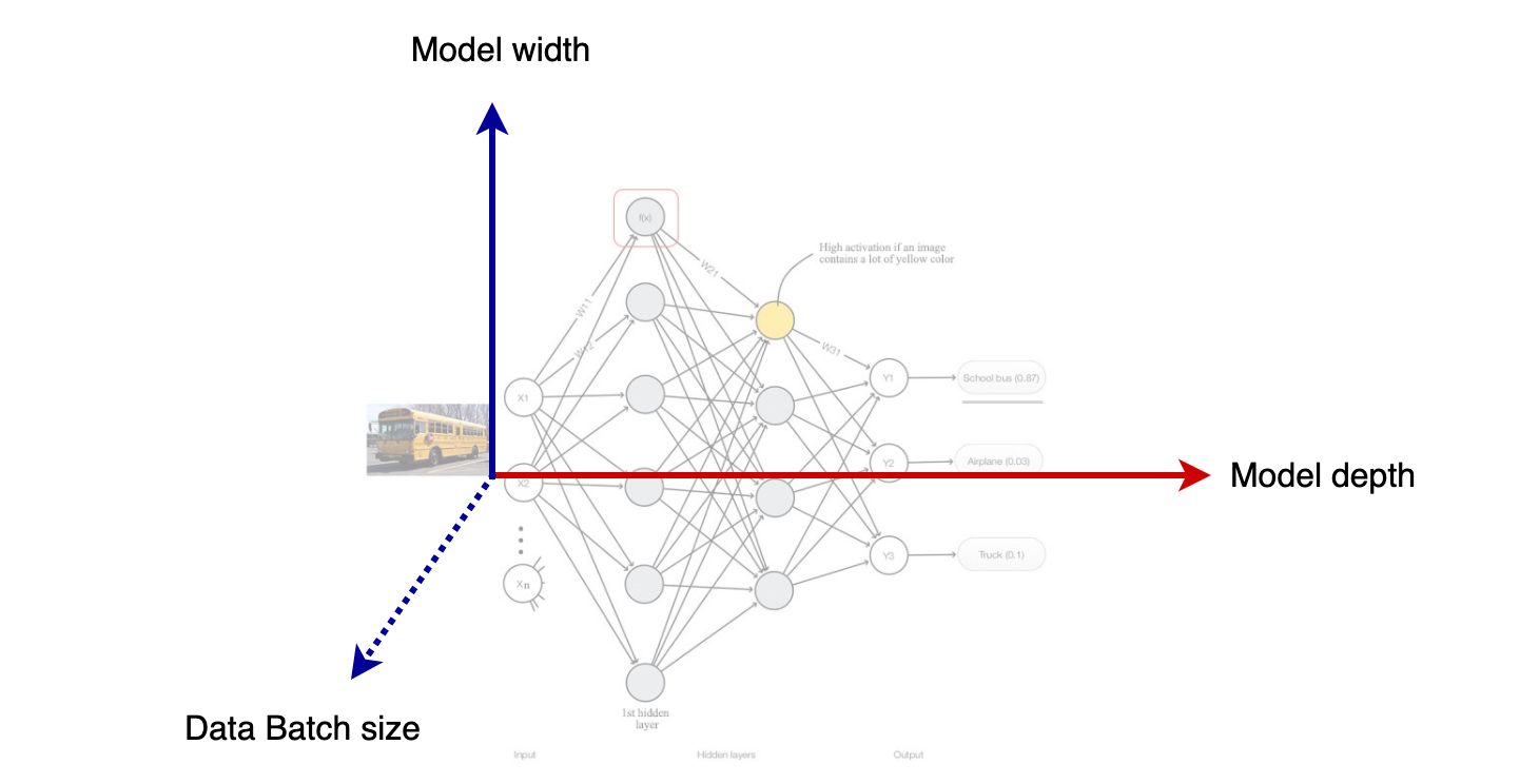
In GPU or TPU, we improve data parallelism for fully connected layers by increasing the batch size. For CNN, we increase parallelism by exploring the filter depth (i.e. the model width).
在GPU或TPU中,我们通过增加批处理大小来改善全连接层的数据并行性。 对于CNN,我们通过探索滤镜深度(即模型宽度)来提高并行度。

But the model depth is not explored by GPU or TPU.
但是GPU或TPU并未探索模型深度。
This leads to a big issue that haunts GPU and TPU designers — the memory bandwidth required to support thousands of concurrent operations. Without a spatial dimension concept, we squeeze all the memory requests into a shared global memory resource. We can think naively that we have a large shared on-chip memory to hold all the input, the activations, and the weights.
这导致困扰GPU和TPU设计人员的一个大问题-支持数千个并行操作所需的内存带宽。 如果没有空间维度的概念,我们会将所有内存请求都压缩到共享的全局内存资源中。 我们可以天真地认为,我们拥有一个共享的大型片上存储器来容纳所有输入,激活和权重。

But this is not practical. Alternatively, the chip designers implement a complex caching scheme to reduce the memory traffic from the off-chip memory. GPU designers spend a lot of effort and die space in addressing this issue. With the hope that if the batch size and filter depth are big enough, the data locality will be sufficient and the problem can be mitigated by caching. Also, the GPU gives developers more memory structures (like SM’s local shared memory) and cache controls. This improves the cache hit ratio significantly. But many startups bet in a different direction — distributed local memory.
但这是不切实际的。 备选地,芯片设计者实施复杂的缓存方案以减少来自片外存储器的存储器流量。 GPU设计人员在解决此问题上花费了大量的精力和精力。 希望如果批处理大小和过滤器深度足够大,则数据局部性将足够,并且可以通过缓存缓解问题。 此外,GPU还为开发人员提供了更多的内存结构(例如SM的本地共享内存)和缓存控件。 这样可以大大提高缓存命中率。 但是许多初创公司押注的方向却不同-分布式本地内存。
There is another mismatch in the programming model. In CPU, instructions read (or write) data in registers coming from (or going) to memory. This enforces a permanent “storage” concept in holding transient calculations. If there is a lot of data, it thrashes the register files or the cache.
编程模型中还有另一个不匹配的地方。 在CPU中,指令读取(或写入)来自(或进入)存储器的寄存器中的数据。 这在进行暂态计算时实施了永久性的“存储”概念。 如果有大量数据,则会破坏寄存器文件或缓存。
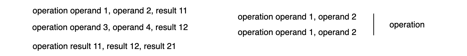
On the contrary, the dataflow in a DL model follows closer to a pipeline model, like the one on the right above (i.e. op1 input | op2 | op3 | op4).
相反,DL模型中的数据流更接近于流水线模型,如右上方(即op1输入| op2 | op3 | op4)。
DL架构 (DL Architecture)
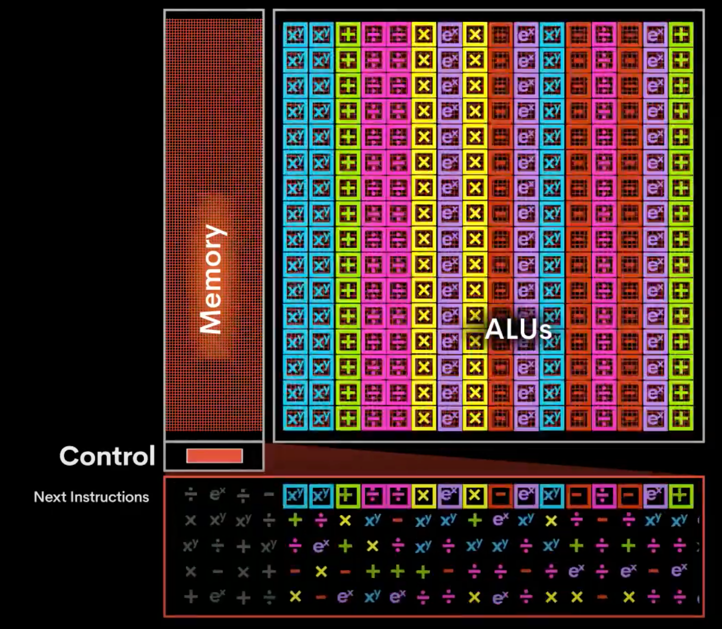
Many hardware designs are instruction focused. But DL is about data volume. If we cannot handle the data movement nicely, not only performance will be hurt but also the power consumption.
许多硬件设计都以指令为重点。 但是DL与数据量有关。 如果我们不能很好地处理数据移动,那么不仅会损害性能,而且会降低功耗。
Let’s consider a new architecture approach that
让我们考虑一种新的架构方法
- can utilize distributed memory in 可以利用分布式内存
- a pipeline structure. 管道结构。

The new design contains an array of cores with distributed memory overlay on top of a network on chip (NoC), say in a mesh configuration. In fact, you will see this often in many startups, just different variants. The cores above are often called tiles. This new architecture reintroduces the spatial structure that puts the model depth back into the equation. Workloads will be run in a pipeline fashion to increase throughput.
新设计包含一组内核,这些内核具有分布在片上网络(NoC)顶部的分布式内存,例如采用网状配置。 实际上,您会在许多初创公司中看到这种情况,只是形式有所不同。 上方的核心通常称为图块 。 这种新的架构重新引入了将模型深度重新纳入方程式的空间结构。 工作负载将以管道方式运行以增加吞吐量。

This array of tiles can be segmented into sub-regions where each region runs a separate DL model. Or a set of tiles can run multiple models for better tile utilization.
瓦片的阵列可以被分割成子区域,其中每个区域运行单独的DL模型。 或者一组图块可以运行多个模型以提高图块利用率。
This pipeline concept is similar to the instruction pipeline in CPU but on the macro scale. CPU instruction execution is carried out in stages. Because each stage is running on different parts of the hardware, instructions can be overlapped. For example, the diagram below shows a hyperthreaded CPU that processes 2 instructions concurrently. With pipelining, it completes 2 instructions for each clock cycle. Without the pipeline, it cannot overlap the instruction execution and finish only 2 instructions in every 5 clock cycles.
该流水线概念类似于CPU中的指令流水线,但在宏观上。 CPU指令执行分阶段执行。 因为每个阶段都在硬件的不同部分上运行,所以指令可以重叠。 例如,下图显示了同时处理2条指令的超线程CPU。 通过流水线处理,每个时钟周期可完成2条指令。 没有流水线,它就不能与指令执行重叠,并且每5个时钟周期只能完成2条指令。

But in any pipes, you don’t want any bottleneck. In our DL situation, this can be worse if the workload assigned to each tile has an un-proportional amount of loads. This causes congestion and lowers tile utilization.
但是在任何管道中,您都不需要任何瓶颈。 在我们的DL情况下,如果分配给每个图块的工作负载具有不成比例的负载,则情况可能更糟。 这导致拥塞并降低瓦片利用率。

Since the DL layer designs and model capacity are known ahead, we can depend on the compiler or the runtime library to assign loads properly. For many startups, they are developing advanced compilers in mapping and scheduling the model layers and nodes computation to this array of tiles.
由于DL层的设计和模型容量是众所周知的,因此我们可以依靠编译器或运行时库来正确分配负载。 对于许多初创公司而言,他们正在开发高级编译器,以将模型层和节点计算映射和调度到此图块阵列。
But there are many variants of this architecture. Many differences are subtle but it makes a big difference. So let’s get into the startups in finding these variants.
但是,此体系结构有许多变体。 许多差异都是细微的,但差异很大。 因此,让我们进入初创公司来寻找这些变体。
图芯 (Graphcore)
Graphcore has a 2nd generation Colossus MK2 IPU processor (GC200) as well as the server IPU-M2000 powered by 4 GC200 IPUs. It also has an IPU-POD configuration with a maximum of 64K IPUs. This achievement is clearly reflected in the company 1.95B valuation on Feb 2020.
Graphcore具有第二代Colossus MK2 IPU处理器(GC200)以及由4个GC200 IPU驱动的服务器IPU-M2000。 它还具有IPU-POD配置,最多支持64K IPU。 2020年2月公司1.95B的估值清楚地体现了这一成就。

Graphcore designs its own IPU (Intelligent Processing Unit) and it is fabricated by TSMC using a 7 nm process. It uses MIMD (Multiple Instruction, Multiple Data) and has 1472 tiles. Similar to TPU and GPU, threads are oversubscribed to tiles to achieve higher utilization. Each tile can run 6 threads (a total of 8832 threads at the IPU level) and it maintains separate hardware context for threads and multiplexes them onto shared resources.
Graphcore设计了自己的IPU(智能处理单元),它是由台积电采用7纳米Craft.io制造的。 它使用MIMD(多指令,多数据),具有1472个图块。 与TPU和GPU相似,线程被超额分配给切片以实现更高的利用率。 每个磁贴可以运行6个线程(在IPU级别上总共为8832个线程),并且为线程维护单独的硬件上下文,并将它们复用到共享资源上。

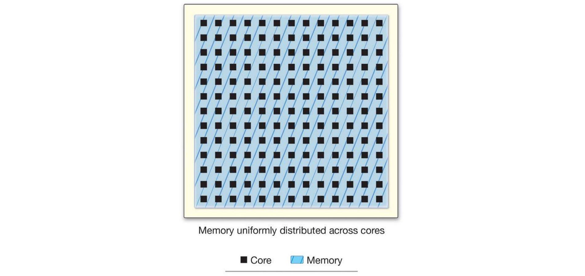
It has 900MB SRAM in-processor-memory (768KB/tile) at 47.5 TB/s. Each tile has its local distributed memory and no global memory is used. With this distributed concept, the developers are responsible for partitioning their working set across the tiles’ memories and make tiles data exchange for non-local operands. But most complexity will be hidden away from developers by the compilers. (Note: some information in this section is originated from a third-party report. It is an excellent source of information for the IPU design but just be careful that the specification is based on its first-generation chip.)
它具有900MB SRAM处理器内存(768KB /块),速度为47.5 TB / s。 每个图块都有其本地分布式内存,并且不使用全局内存。 利用这种分布式概念,开发人员负责在图块的内存之间划分其工作集,并使图块数据交换为非本地操作数。 但是编译器会将大多数复杂性对开发人员隐藏起来。 (注意:本节中的某些信息来自第三方报告 。它是IPU设计的极好信息来源,但请注意,该规范基于其第一代芯片。)
The IPU supports FP32, FP16.32 (16bit multiply-32bit accumulate), FP16.16 (16bit multiply-accumulate), and stochastic rounding. According to Graphcore, this allows them to keep all arithmetic in 16-bit formats. It is also optimized for model sparsity. IPU cores provide more complex functions than GPU’s SMs. It pays no penalty for branch divergence. Also, each tile can generate a separate random number seed needed for ML algorithms like evolution models.
IPU支持FP32,FP16.32(16位乘以32位累加),FP16.16(16位乘以累加)和随机舍入。 根据Graphcore的说法,这使他们可以将所有算术保持为16位格式。 它还针对模型稀疏性进行了优化。 IPU内核提供的功能比GPU的SM更复杂。 它不为分支分歧付出任何代价。 而且,每个图块都可以生成ML算法(例如演化模型)所需的单独的随机数种子。
Tiles are connected in an all-to-all fashion — any tiles can communicate to any tile in the IPU with short latency. It has 10 IPU link interfaces (video) to support high-bandwidth 320GB/s communications among the IPUs. These factors allow fast memory access in the remote IPUs but more importantly, the high-speed connection transforms a cluster of IPU into a single node. This allows us to map a large DNN easily. It also has 2 PCIe Gen4 for communication with the CPU host.
磁贴以全包方式连接-任何磁贴都可以与IPU中的任何磁贴进行短时通信。 它具有10个IPU链接接口( 视频 ),以支持IPU之间的高带宽320GB / s的通信。 这些因素允许在远程IPU中快速访问内存,但更重要的是,高速连接将IPU群集转换为单个节点。 这使我们能够轻松映射大型DNN。 它还具有2个PCIe Gen4,用于与CPU主机通信。
Graphcore uses its Poplar software system to deploy applications to servers. This quote from Graphcore is a good summary of the role of the compiler in this new architecture.
Graphcore使用其Poplar软件系统将应用程序部署到服务器。 Graphcore的这段引文很好地总结了编译器在这种新架构中的作用。
You can use your preferred AI framework, such as TensorFlow or PyTorch, and from this high-level description, Poplar will build the complete compute graph, capturing the computation, the data and the communication. It then compiles this compute graph and builds the runtime programs that manage the compute, the memory management and the networking communication, to take full advantage of the available IPU hardware.
您可以使用首选的AI框架(例如TensorFlow或PyTorch),并且从此高级描述中,Poplar将构建完整的计算图,捕获计算,数据和通信。 然后,它会编译此计算图并构建用于管理计算,内存管理和网络通信的运行时程序,以充分利用可用IPU硬件。

大脑 (Cerebras)
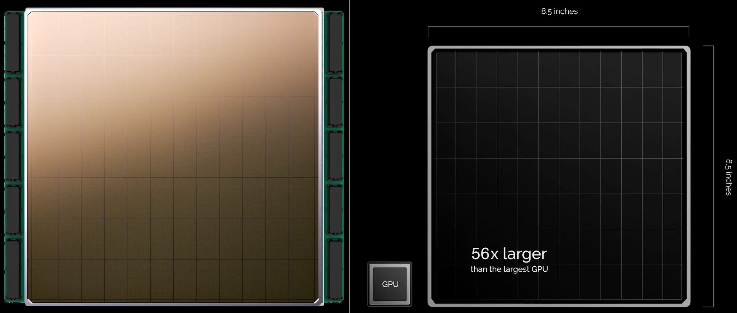
SoC (System on a chip) packs the majority of computer components on a single die which is later packaged onto a chip. But why do we stop our imagination there? In DL, we utilize a cluster of nodes in training complex DL models. Instead of cutting the dies off from the wafer, Cerebras builds a cluster of systems on a single wafer. That is the key idea behind Cerebras Wafer Scale Engine (WSE).
SoC(片上系统)将大多数计算机组件封装在一个芯片上,然后再封装到芯片上。 但是为什么我们在这里停止想象呢? 在DL中,我们在训练复杂的DL模型中利用了节点簇。 Cerebras并未从晶片上切下裸片,而是在单个晶片上构建了一组系统。 这是Cerebras晶圆规模引擎(WSE)背后的关键思想。
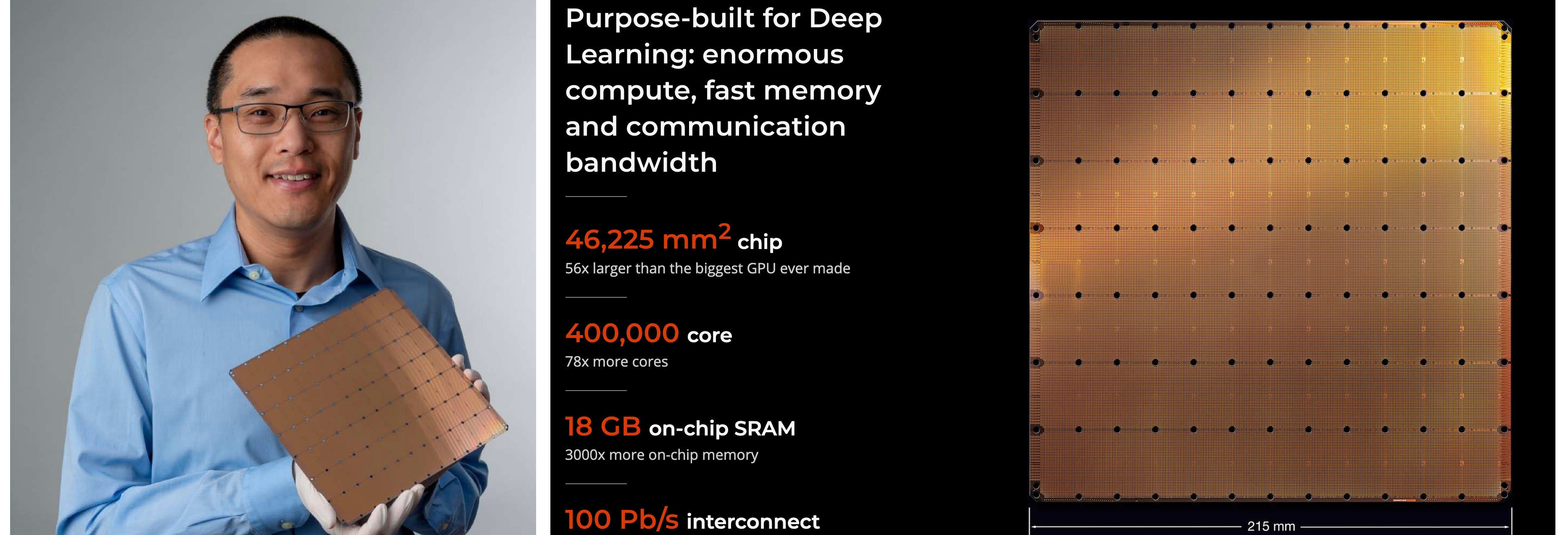
This wafer contains 84 “chips” (as shown above as 7×12), a total of 400K cores, and 18GB on-chip memory.
该晶圆包含84个“芯片”(如上图所示为7×12),总共40万个内核和18GB的片上内存。
In standard chip fabrication, scribe lines separate each die for later cutting.
在标准芯片制造中,划片线将每个管芯分开以供以后切割。

In WSE, wires are added on top of the scribe lines to form a 2D mesh network. Communication is done directly by hardware with small single-word messages. This network achieves 100 Pb/s ultra-high bandwidth with short latency. In fact, there is no difference between the connectivity between cores and across scribes. The whole wafer can be viewed as a large array of cores.
在WSE中,将导线添加到划线的顶部以形成2D网格网络。 硬件直接通过小的单字消息进行通信。 该网络以短延迟实现了100 Pb / s的超高带宽。 实际上,核心之间和抄写员之间的连接没有区别。 整个晶圆可以看作是一大堆芯。

WSE contains 400K cores handling general instructions including arithmetic, logical, load/store, and branch operations. It also includes tensor operations for DL acceleration. Each core is run independently of others. It allows heterogeneous workloads to be run on the cores concurrently.
WSE包含40万个内核,可处理常规指令,包括算术,逻辑,加载/存储和分支操作。 它还包括用于DL加速的张量运算。 每个核心独立于其他核心运行。 它允许异构工作负载在内核上同时运行。

For each core, multiple operations can be run concurrently and cores can work in parallel in handling one layer. WSE also adopts distributed memory that spread over the wafer without a central memory.
对于每个内核,可以同时运行多个操作,并且内核可以并行处理一层。 WSE还采用了分布在整个晶圆上的分布式内存,而没有中央内存。
The whole DNN will be mapped and run on a single wafer. This takes advantage of the large on-chip memory as well as the high-bandwidth and low-latency communication between cores at the silicon level.
整个DNN将被映射并在单个晶片上运行。 这利用了大的片上存储器以及芯片级内核之间的高带宽和低延迟通信。
The Cerebras Graph Compiler (CGC) translates the DNN to an optimized WSE executable. Kernels corresponding to each DNN layers are sized. More complex workloads will be assigned with larger groups of cores. CGC then generates a placement and routing to minimize communication latency between the layers. (Polyhedral compilation techniques are applied here.)
Cerebras Graph Compiler(CGC)将DNN转换为优化的WSE可执行文件。 调整与每个DNN层相对应的内核的大小。 将为更复杂的工作负载分配更大的内核组。 CGC然后生成一个布局和路由,以最小化各层之间的通信延迟。 (这里应用了多面体编译技术。)

The DL model is extracted from standard frameworks and convert to the Cerebras Linear Algebra Intermediate Representation (CLAIR).
DL模型是从标准框架中提取的,并转换为Cerebras线性代数中间表示(CLAIR)。

I will quote directly from here for its compiler strategy. It explains more details on the tasks and the requirement of the compiler. (The massive array of cores are referred to as compute fabric here.)
我将直接从此处引用其编译器策略。 它解释了有关任务和编译器要求的更多详细信息。 (大量的内核在这里称为计算结构。)
CGC performs a matching and covering operation that matches subgraphs to kernels from the Cerebras kernel library. These kernels are optimized to provide high-performance compute at extremely low latency on the fabric of the WSE. The result of this matching operation is a kernel graph.
CGC执行匹配和覆盖操作,将子图与Cerebras内核库中的内核进行匹配。 这些内核经过优化,可在WSE架构上以极低的延迟提供高性能计算。 该匹配操作的结果是内核图。
Using its knowledge of the unique WSE architecture, CGC then allocates compute and memory to each kernel in the graph and maps each kernel onto a physical region of the computational array of cores. Finally, a communication path, unique to each network, is configured onto the fabric.
利用其对独特WSE体系结构的了解,CGC然后将计算和内存分配给图中的每个内核,并将每个内核映射到内核计算阵列的物理区域。 最后,将每个网络独有的通信路径配置到结构上。
…
…
During this compilation process, kernel placement is formulated as a multi-constraint problem on 1) memory capacity and bandwidth, 2) computation requirements, and 3) communication costs. The placement engine takes into account both algorithmic efficiency and compute core utilization to generate a result that maximizes locality, minimizes communication requirements, and avoids hotspots and contention. The final result is a CS-1 executable, ...
在此编译过程中,内核放置被表述为以下方面的多约束问题:1)内存容量和带宽,2)计算要求和3)通信成本。 放置引擎同时考虑了算法效率和计算核心利用率,以生成使局部性最大化,通信需求最小化并避免热点和争用的结果。 最终结果是CS-1可执行文件,...
The core can process sparse models natively in hardware for high speedup. The dataflow and computation are triggered by data. Zero data branches are filtered out to avoid unnecessary processes. Because cores run independently, the dataflow can run continuously whenever possible without synchronizing with other cores.
内核可以在硬件中本地处理稀疏模型,以提高速度。 数据流和计算由数据触发。 零数据分支被过滤掉以避免不必要的处理。 由于内核独立运行,因此数据流可以在任何可能的情况下连续运行,而无需与其他内核同步。

Manufacture Challenges (Optional)
制造挑战(可选)
Using a whole wafer to build a system has been attempted before AI chips. But there are many challenges that need to solve including manufacturing yield, thermal expansion on the package, package assembly, and power and cooling. Cerebras solves them by adding fault tolerance design, developing custom connectors between layers (top right below), and customizing new packaging tools for precise alignment. To cool the silicon, a cold plate is placed on top, and power is supplied underneath it.
在AI芯片之前,已经尝试使用整个晶圆来构建系统。 但是,还需要解决许多挑战,包括制造良率,封装上的热膨胀,封装组装以及电源和冷却。 Cerebras通过添加容错设计,开发各层之间的自定义连接器(下面右上方)以及自定义新的包装工具以进行精确对准来解决这些问题。 为了冷却硅,在其顶部放置一个冷却板,并在其下方供电。

Specification (Optional)
规格(可选)
Here is the general information available from a third-party source. In this article, we will present some high-level specifications. Feel free to skip or browse through them according to your interest.
以下是可从第三方来源获得的常规信息。 在本文中,我们将介绍一些高级规范。 可以根据自己的兴趣随意跳过或浏览它们。

格罗克 (Groq)
Here is a nice video summarizing the design concept of the Groq’s Tensor Streaming Processor (TSP).
这是一个很好的视频,总结了Groq的Tensor流处理器(TSP)的设计概念。
As demonstrated from the video, it has a slightly different pipeline structure. The pipeline moves from the left to the right in which cores in the same column execute the same instruction (SIMD).
如视频所示,它的管道结构略有不同。 流水线从左向右移动,同一列中的内核执行同一条指令(SIMD)。
The majority of the control logic and cache is gone. It strongly depends on the compiler and the host in issuing instructions.
大多数控制逻辑和缓存都消失了。 在发布指令时,它很大程度上取决于编译器和主机。
As quoted from Groq,
正如Groq所说,
Instead of creating a small programmable core and replicating it dozens or hundreds of times, the TSP houses a single enormous processor that has hundreds of functional units. This novel architecture greatly reduces instruction-decoding overhead, and handles integer and floating-point data, which makes delivering the best accuracy for inference and training a breeze.
TSP并没有创建一个小的可编程核心并将其复制数十或数百次,而是拥有一个具有数百个功能单元的巨大处理器。 这种新颖的体系结构极大地减少了指令解码的开销,并处理整数和浮点数据,这使得为推理和训练提供最佳的准确性变得轻而易举。
Again, this design depends on the compiler in optimizing how instructions are issued.
同样,这种设计取决于编译器来优化指令的发布方式。
神话 (Mythic)

Mythic chips are tile-based that features three fundamental hardware technologies:
神话般的芯片基于图块,具有三种基本硬件技术:
- Compute-in-memory, 内存计算
- Dataflow architecture and 数据流架构和
- Analog computing. 模拟计算。
We discuss the first two concepts already. So we will be brief. The first one uses localized memory.
我们已经讨论了前两个概念。 因此,我们将简短介绍。 第一个使用本地化的内存。

The second one uses the dataflow concept to run the DNN graph.
第二个使用数据流概念来运行DNN图。

As quoted from Mythic, this is how the pipeline works with a little bit more detail.
正如Mythic所引用的那样,这就是管道如何工作的更多细节。
When the results from one graph node are completed, they flow to the next graph node to start the next operation, which is ideal for dataflow architecture. In our dataflow architecture, we assign a graph node to each compute-in-memory array and put the weight data for that graph node into that memory array. When the input data for that graph node is ready, it flows to the correct location, adjacent to the memory array, and then is executed upon by the local compute and memory.
当一个图节点的结果完成后,它们将流到下一个图节点以开始下一个操作,这是数据流体系结构的理想选择。 在我们的数据流体系结构中,我们将一个图节点分配给每个内存中计算数组,并将该图节点的权重数据放入该内存数组中。 当该图节点的输入数据准备就绪时,它会流到与内存阵列相邻的正确位置,然后由本地计算和内存执行。
Our dataflow architecture also maximizes inference performance by having many of the compute-in-memory elements operating in parallel, pipelining the image processing by processing neural networks nodes (or “layers”) in parallel in different parts of the frame.
我们的数据流体系结构还通过使许多内存中计算元素并行运行,通过在帧的不同部分中并行处理神经网络节点(或“层”)来流水处理图像处理,来最大化推理性能。

Their third innovation is quite interesting. Instead of using a digital circuit design, it tunes the value of resistors according to weights and uses the input value to control the voltage. The output current will determine the computation result. Here are the details from Mythic.
他们的第三项创新非常有趣。 它没有使用数字电路设计,而是根据权重来调整电阻器的值,并使用输入值来控制电压。 输出电流将确定计算结果。 这是Mythic的详细信息。
Our analog compute takes compute-in-memory to an extreme, where we compute directly inside the memory array itself. This is possible by using the memory elements as tunable resistors, supplying the inputs as voltages and collecting the outputs as currents. We use analog computing for our core neural network matrix operations, where we are multiplying an input vector by a weight matrix.
我们的模拟计算将内存中的计算发挥到了极致,我们可以在内存阵列本身内部直接进行计算。 通过将存储元件用作可调电阻器,将输入提供为电压并将输出收集为电流,可以实现此目的。 我们将模拟计算用于核心神经网络矩阵运算,其中我们将输入向量乘以权重矩阵。
First, it is amazingly efficient; it eliminates memory movement for the neural network weights since they are used in place as resistors. Second, it is high performance; there are hundreds of thousands of multiply-accumulate operations occurring in parallel when we perform one of these vector operations.
首先,它效率极高; 由于它们被用作电阻器,因此消除了神经网络权重的内存移动。 其次,它是高性能的; 当我们执行这些向量运算之一时,并行发生数十万次乘法累加运算。
海洛 (Hailo)

Hailo applies pipeline architecture using distributed memory also. But it focuses on the edge device for inference.
Hailo也使用分布式内存来应用管道架构。 但它着重于边缘设备进行推理。
By moving the memory closer to the core, it allows for very low power consumption for the edge device. This is a nice animation on how DNN is mapped into a resource graph that eventually mapped into the processor cores.
通过将内存移至靠近内核的位置,它可以使边缘设备的功耗非常低。 这是一个很好的动画,说明了如何将DNN映射到资源图,该资源图最终映射到处理器内核。

更多 … (More …)
This is Part 1 of the “AI Chips Technology Landscape”. There are plenty more for our discussion. In part 2, we. want to discuss SambaNova founded in 2017. It is one mystical AI chip company with about half a billion VC investment. But their approach can be quite revolutionary, except no outsiders know what exactly it is. But that does not mean we cannot put on our investigation hats. In fact, we will go deep in looking at the co-founders’ researches at Stanford.
这是“ AI芯片技术前景”的第1部分。 还有很多我们需要讨论的地方。 在第2部分中,我们。 想要讨论成立于2017年的SambaNova。这是一家神秘的AI芯片公司,拥有大约十亿VC的投资。 但是他们的方法可能是非常革命性的,除非没有外界知道它到底是什么。 但这并不意味着我们不能戴上调查帽。 实际上,我们将深入研究斯坦福大学联合创始人的研究。
ai芯片fpga


 被折叠的 条评论
为什么被折叠?
被折叠的 条评论
为什么被折叠?
 到【灌水乐园】发言


