东莞理工大学计算机专业是一本吗,东莞这一所大学,教学质量不断提高,您听说过吗?...

本文介绍了东莞理工学院的莞城和松山湖校区,重点解析了该校的三个王牌专业:软件工程、计算机类(包括计算机科学与技术)和机械专业。软件工程卓越班对学生要求严格,不合格者将淘汰回普通班级。机械专业因其优秀师资,如校长马宏伟教授,以及硕士专业学位授权点的设立,显示出其学术实力。文章指出,虽然高考竞争激烈,但大学期间的自我管理也至关重要,未来掌握在自己手中。

摘要生成于 C知道 ,由 DeepSeek-R1 满血版支持, 前往体验 >

文 | 微谈教育

文章原创,版权归作者所有,欢迎点赞评论。

东莞理工学院,有两个校区,一个位于东莞莞城,称为莞城校区,另外一个校区位于东莞市松山湖区,临近华为小镇。

ace0b5a5261bf45b3bebcd2cac34edaf.png

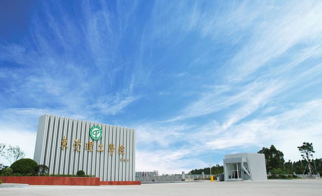
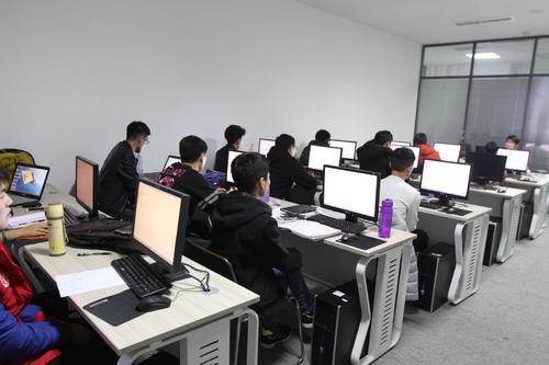
东莞理工学院松山湖校区,基本上集中了整个学校的教学资源,是东莞市内一个不错的高水平大学。

2020年的高考志愿填报之后,东莞理工学院也公布出来2020年招生的基本情况。

406cd67602c02a5d9bb8264a311f5920.png

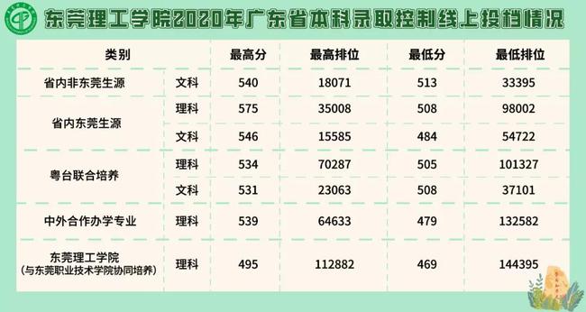
在学校所给出的投档情况上来看,省内非东莞理科生源,一次性满档,所录取的学生,都是高分优投线以上。

22e45ade10e117028c0f3f7e41675680.png

东莞生源比非东莞生源所录取的分数要低得多,这是学校给东莞生源的优惠。莞工为地方性大学,自然会给本地的高考生们以降分录取。

像深圳大学一样,对于深圳的生源,同样是给予降分录取。

这里的“降分录取”,是学校给予东莞生源一定的名额,报考的人数,数量少,因此比省内的非东莞生源分数线低。

77dfb485d83be780db18477cc66370cf.png

东莞理工学院,从录取的分数线来看,是一所刚过一本线的理工科大学。在这所大学当中,也有几个王牌专业,整个学校最优秀的资源,集中在这几个专业当中。

一、软件工程专业

一所理工科的大学,必不可少,一定会有计算机的专业。莞工的软件工程专业,是学校录取分数最高的专业之一,一般会超过高分优投线三十分左右。

在软件工程专业的基础之上,再设立软件工程卓越班,从报考软件工程专业的学生当中,排名录取两个班的学生,进入软件工程卓越班。

75fef9ca60e2c2bc2f7a449d69dad453.png

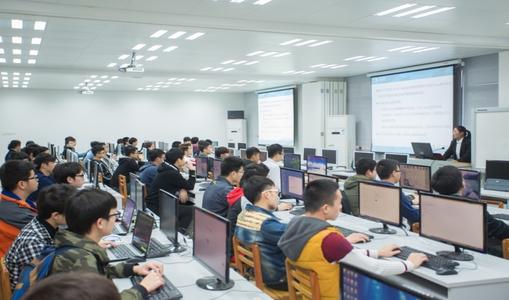
在每一年的期末考试中,会对软卓的同学们进行考核,不合格的同学,将会被淘汰下来,回到软件工程班。

软件工程卓越班,是整个学校录取最高分的班级之一,是名副其实的一本专业。

二、计算机类专业

计算机类专业,在2018年之前,命名为计算机科学与技术专业,到2019年,学校对专业进行改革,把名字改为“计算机类专业”。

a083e371d6be9b0be93c66ce0180b513.png

软件工程专业,是从计算机类专业分支出去,只不过软件工程专业学生所学的专业知识,分得更细。

大体上,两个专业的专业方向,还是会有异曲同工之处,所涉及到的专业知识,大体上是相同的。

三、机械专业

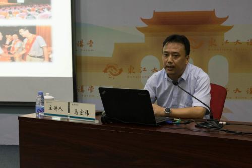
机械专业,同样也是东莞理工学院的王牌专业之一。在2020年,机械专业被设立为东莞理工学院的硕士专业学位授权点。

其中机械专业的导师,马宏伟教授,是东莞理工学院的校长,曾经参与建设港珠澳大桥的设计工作。

774f6adf5f8cb4dc27550b2d4e8a6509.png

这三个专业,是这所大学比较出名的专业。当然,过了高考这一关,还有大学。虽说高考是千军万马过独木桥,大学四年又何尝不是。

只不过,大学四年比较自由,学校、老师、家长限制得比较少,就靠学生们的自律。未来,还是要把握在自己的手上的。

作者:微谈教育,欢迎关注。文章图片来源于网络,如果侵权,请联系删除。

### QSPI Controller IP Configuration and Implementation in FPGA or ASIC Design In the context of configuring and implementing a QSPI (Quad Serial Peripheral Interface) controller IP within an FPGA or ASIC design, several key aspects must be considered to ensure proper functionality. While logic analyzers provide detailed analysis capabilities for protocols like SPI through scope-based triggering and protocol decoding [^1], these tools are not directly involved in the configuration process but can assist during debugging phases. #### Understanding QSPI Protocol The QSPI interface extends standard SPI by supporting up to four data lines allowing simultaneous transmission and reception which significantly increases throughput compared to traditional SPI interfaces that only use one MISO/MOSI line per transaction. This feature makes it particularly suitable for high-speed memory access applications such as flash memories where fast read/write operations are required. #### Configuring QSPI Controller IP When integrating a QSPI controller into either FPGAs or ASICs, designers need to focus on setting parameters related to clock frequency, mode bits, dummy cycles count, address length, instruction set used for communication commands among others depending upon specific requirements: - **Clock Frequency**: Determines how quickly transactions occur over the bus. - **Mode Bits**: Define whether the device operates in single/dual/quad modes along with polarity settings. - **Dummy Cycles Count & Address Length**: These depend heavily on connected devices' specifications ensuring correct timing between command issuance and actual data transfer initiation. For instance, when working with Xilinx Vivado HLS toolchain targeting Zynq Ultrascale+ MPSoC parts, users would configure these properties using TCL scripts provided alongside core instantiation templates. ```tcl set_property CONFIG.C_S_AXI_QSPI_BASEADDR {0x80000000} [get_bd_cells axi_qspi_0] set_property CONFIG.C_SPI_MEMORY_TYPE {QSPI_FLASH} [get_bd_cells axi_qspi_0] set_property CONFIG.C_NUM_TRANSFER_BITS {32} [get_bd_cells axi_qspi_0] ``` This script snippet sets base address mapping, specifies target memory type as quad SPI Flash, and defines number of transferred bits accordingly. #### Implementing QSPI Controller Logic Within Hardware Description Language Code To implement custom functionalities beyond what pre-built IPs offer, writing HDL code becomes necessary. Below shows part of Verilog module defining state machine controlling different states during write operation sequence including sending opcode followed by addresses then finally transferring payload bytes. ```verilog module qspi_controller ( input wire clk, output reg [7:0] sdo_data, ... ); // State definitions typedef enum { IDLE, SEND_OPCODE, TRANSFER_ADDR, WRITE_DATA } state_t; state_t current_state; integer addr_counter = 0; // Used while transmitting multiple byte addresses always @(posedge clk) begin : proc_current_state case(current_state) IDLE: if(start_write_signal) begin current_state <= SEND_OPCODE; end SEND_OPCODE: begin sdo_data <= OP_CODE_WRITE; current_state <= TRANSFER_ADDR; end TRANSFER_ADDR: if(addr_counter < ADDR_WIDTH_IN_BYTES) begin sdo_data <= address_reg[addr_counter*8+:8]; addr_counter++; end else begin current_state <= WRITE_DATA; end WRITE_DATA: /* Handle Data Transfer */ endcase end ... endmodule ``` --related questions-- 1. What considerations should be taken into account when selecting a QSPI controller IP? 2. How does the choice of operating mode affect performance characteristics in QSPI communications? 3. Can you explain more about error handling mechanisms implemented inside typical QSPI controllers? 4. In terms of power consumption optimization, what strategies could apply specifically towards designing efficient QSPI systems?
评论
添加红包

请填写红包祝福语或标题

红包个数最小为10个

红包金额最低5元

当前余额3.43前往充值 >
需支付:10.00
成就一亿技术人!
领取后你会自动成为博主和红包主的粉丝 规则
hope_wisdom
发出的红包
实付
使用余额支付
点击重新获取
扫码支付
钱包余额 0

抵扣说明:

1.余额是钱包充值的虚拟货币,按照1:1的比例进行支付金额的抵扣。
2.余额无法直接购买下载,可以购买VIP、付费专栏及课程。

余额充值