


http://infocenter.arm.com/help/index.jsp?topic=/com.arm.doc.dui0499b/BEHEIHCE.html
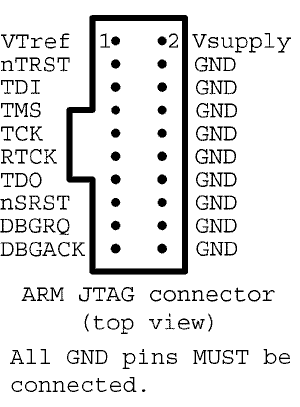
he ARM JTAG 20 connector is a 20-way 2.54mm pitch connector.
It can be used in either standard JTAG (IEEE 1149.1) mode or Serial Wire Debug (SWD) mode.
The following figure shows the ARM JTAG 20 connector pinout:
The following table describes the signals on the ARM JTAG 20 interfaces:
Table 7. ARM JTAG 20 signals
| Signal | I/O | Description |
|---|---|---|
| TDI | Output | The Test Data In pin provides serial data to the target during debugging. TDIcan be pulled HIGH on the target. |
| TDO | Input | The Test Data Out pin receives serial data from the target during debugging. You are advised to series terminate TDO close to the target processor. TDO is typically pulled HIGH on the target. |
| TMS | Output | The Test Mode Select pin is used to set the state of the Test Access Port (TAP) controller on the target. TMS can be pulled HIGH on the target to keep the TAP controller inactive when not in use. |
| TCK | Output | The Test Clock pin is used to clock data into the TDI and TMS inputs of the target. TCK is typically pulled HIGH on the target. |
| RTCK | Input | The Return Test Clock pin is used to echo the test clock signal back to DSTREAM for use with adaptive mode clocking. If RTCK is generated by the target processor, you are advised to series terminate it. RTCK can be pulled HIGH or LOW on the target when not in use. |
| nTRST | Output | The Test Reset pin can be used to reset the TAP controller of the processor to allow debugging to take place. nTRST is typically pulled HIGH on the target and pulled strong-LOW by DSTREAM to initiate a reset. The polarity and strength of nTRST is configurable. |
| nSRST | Input/Output | The System Reset pin is used to fully reset the target. This signal can be initiated by DSTREAM or by the target board (which is then detected by DSTREAM). nSRST is typically pulled HIGH on the target and pulled strong-LOW to initiate a reset. The polarity and strength of nSRST is configurable. |
| DBGRQ | Output | The Debug Request pin can be used to stop the target processor and put it into debug state. DBGRQ is rarely used by current systems and is usually pulled LOW on the target. |
| DBGACK | Input | The Debug Acknowledge pin can be used to notify DSTREAM that a debug request has been received and the target processor is now in debug state. DBGACK is rarely used by current systems and is usually pulled LOW on the target. |
| SWDIO(TMS) | Input/Output | The Serial Wire Data I/O pin sends and receives serial data to and from the target during debugging. You are advised to series terminate SWDIO close to the target processor. |
| SWCLK(TCK) | Output | The Serial Wire Clock pin clocks data into and out of the target during debugging. |
| SWO (TDO) | Input | The Serial Wire Output pin can be used to provide trace data to DSTREAM. You are advised to series terminate SWO close to the target processor. |
| VTREF | Input | The Voltage Target Reference pin supplies DSTREAM with the debug rail voltage of the target to match its I/O logic levels. VTREF can be tied HIGH on the target. If VTREF is pulled HIGH by a resistor, its value must be no greater than 100Ω. |
| VSUPPLY | Input | It is reserved for compatibility with other equipment.Connect to Vdd or leave open in target system. |
| GND | - | Ground. |


 3万+
3万+

 被折叠的 条评论
为什么被折叠?
被折叠的 条评论
为什么被折叠?
 到【灌水乐园】发言


