


实现一个简易的五级流水的CPU,解决Hazard,并实现板极验证。
1 设计总览
2 实现原理
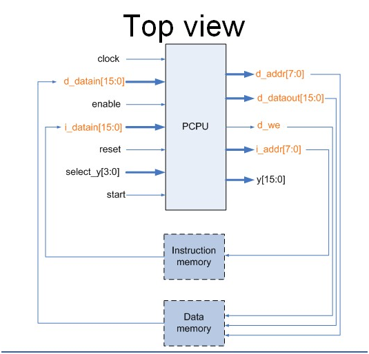
根据Top view 将整个CPU分为3个模块:
1 PCPU 主要模块:用从指令内存得到的指令进行运算处理,并从数据内存中写入或读取数据。这是最核心的部分,其他模块都很好设计。
2 Instruction_Mem 指令模块: 为PCPU模块提供指令,使得PCPU中通过指令寄存器中的值,找到指令的内存地址,从而读取指令。
3 Data_Mem 数据模块: PCPU从中读取数据或写入数据
板极验证:
用4个开关表示选择哪一个数据显示,用4个7段数码管显示数字
3 整个PCPU的工作流程:
五级流水:
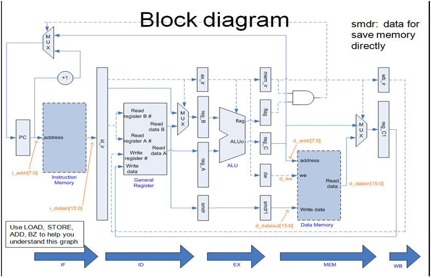
注释:
IF : 从指令模块中,通过指令寄存器PC寻址,获得指令。
ID: 解码指令,根据操作码提取要用到的数据输入通用寄存器。
EX: ALU运算单元在指令的调度下,使用之前通用寄存器中的数据根据不同指令完成不同运算。运算后将结果输出到reg_C中,并设置各个标记位的值。
MEM:这里主要是针对LOAD,STORE这类的读写指令要用到的。对于其他指令没有特别要求。
WB:回写把计算结果写入指令的左值中,这里除了跳转指令和load,store指令,都是写回第一个操作数(寄存器)
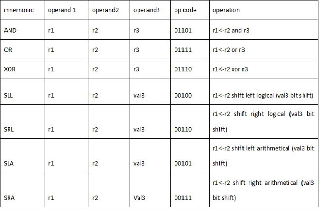
4 需要实现的汇编指令


5 分阶段实现优化过程
阶段一 : 实现最基本的cpu(没有指令存储器,数据存储器,没有解决hazard,没有板极验证,什么也没有…)
完成步骤:
步骤1:理解流水线工作原理
上课时流水线是听懂了,寄存器赋值,取数这些基本原理大概弄懂了。不过实际操作还是有很多要注意的。
步骤2:开始逐级编写基本代码
有了老师给的样例代码,整个框架基本构建好了。所以要做的就是弄清楚每个指令在每一级流水中需要做些什么,然后在每一级流水中再总结这些操作的共同点,不同点,需要特别注意的地方。
1)指令操作码的设计:
优化:这里考虑了一下控制指令的特殊性,因为控制指令在流水每一级操作中有很大相似性,所以为了简化电路,还有判断时代码的简化,把所有控制指令的前两位设为“11”,而其他指令前两位都不是“11”。这样编写代码的时候更容易理清逻辑,综合的时候电路也简单一些。
2)指令各级流水的设计:
这里思考了很多,设计每一条指令都需要特别小心,最重要的是在ID和EX还有ALUo中。
总结一下,主要就是整个16 bits的指令在流水线的每一步中起到“指挥”作用,然后每一级流水的工作就是在上一级完成后,利用
A ID中的寄存器赋值:
reg_A 和 reg_B中存储的是在指令右边将要送入ALU参与运算的值。
由于指令的右边通常声明的是寄存器的编号(因为用户只能对通用寄存器进行操作,无法直接访问内存)或者立即数,所以要通过编号找到确定的寄存器,再将该通用寄存器里的值赋给reg_A 或者 reg_B。
优化: 这里为了减少reg_A 和 reg_B的翻转,考虑了一些优化。比如把要用到立即数的指令的立即数不写入寄存器,而是在下一级流水中之间从指令中取数。
B ex中ALUo的计算
主要就是用verilog本身的运算直接操作。运算后赋值个ALUo寄存器和cf标志位。
优化:比如一些用立即数的操作,之前没有存入reg_A 和 reg_B,直接从ex_ir中取数计算。
C mem中的读写
主要要和data模块进行数据传输,指令就是load和store。
D wb中写回运算结果
由于算数指令和逻辑运算指令基本都是要写回到寄存器。所以这里判断为:非跳转指令,非store,load指令,则写回第一个操作数(寄存器)。
6 源代码
1).v
`timescale 1ns / 1ps
//
// Company:
// Engineer:
//
// Create Date:    14:15:05 12/18/2014
// Design Name:
// Module Name:    CPU
// Project Name:
// Target Devices:
// Tool versions:
// Description:
//
// Dependencies:
//
// Revision:
// Revision 0.01 - File Created
// Additional Comments:
//
//
// data transfer & Arithmetic
`define NOP 5'b00000
`define HALT 5'b00001
`define LOAD 5'b00010
`define STORE 5'b00011
`define LDIH 5'b10000
`define ADD 5'b01000
`define ADDI 5'b01001
`define ADDC 5'b10001
`define SUB 5'b01011
`define SUBI 5'b10011
`define SUBC 5'b10111
`define CMP 5'b01100
// control
`define JUMP 5'b11000
`define JMPR 5'b11001
`define BZ 5'b11010
`define BNZ 5'b11011
`define BN 5'b11100
`define BNN 5'b11101
`define BC 5'b11110
`define BNC 5'b11111
// logic / shift
`define AND 5'b01101
`define OR 5'b01111
`define XOR 5'b01110
`define SLL 5'b00100
`define SRL 5'b00110
`define SLA 5'b00101
`define SRA 5'b00111
// general register
`define gr0  3'b000
`define gr1  3'b001
`define gr2  3'b010
`define gr3  3'b011
`define gr4  3'b100
`define gr5  3'b101
`define gr6  3'b110
`define gr7  3'b111
// FSM
`define idle 1'b0
`define exec 1'b1

/******* the whole module CPU is made of  Instuction_Mem module, PCPU module and Data_Mem module ********/
module CPU(
    input wire clk, clock, enable, reset, start,
	 input wire[3:0] select_y,
	 output [7:0] select_segment,
	 output [3:0] select_bit
    );

wire[15:0] d_datain;
wire[15:0] i_datain;
wire[7:0] d_addr;
wire[7:0] i_addr;
wire[15:0] d_dataout;
wire d_we;
wire[15:0] y;

reg [20:0] count = 21'b0;


	Instruction_Mem instruction(clock,reset,i_addr,i_datain);
	PCPU pcpu(clock, enable, reset, start, d_datain, i_datain,
	 select_y, i_addr, d_addr, d_dataout, d_we, y);


	Data_memory data(clock, reset, d_addr, d_dataout, d_we, d_datain);

   Board_eval eval(clk, y, select_segment, select_bit);
endmodule

/************************ Instruction memeory module   *****************************/
module Instruction_Mem (
    input wire clock, reset,
    input wire[7:0] i_addr,
	output [15:0] i_datain
	 );
reg[15:0] i_data[255:0]; // 8 bits pc address to get instructions
reg[15:0] temp;

always@(negedge clock)
begin
	if(!reset)
	    begin
	       i_data[0] <= {`LOAD, `gr1, 1'b0, `gr0, 4'b0000};
		    i_data[1] <= {`LOAD, `gr2, 1'b0, `gr0, 4'b0001};
		    i_data[2] <= {`ADD, `gr3, 1'b0, `gr1, 1'b0, `gr2};
		    i_data[3] <= {`SUB, `gr3, 1'b0, `gr1, 1'b0, `gr2};
		    i_data[4] <= {`CMP, `gr3, 1'b0, `gr2, 1'b0, `gr1};
		    i_data[5] <= {`ADDC, `gr3, 1'b0, `gr1, 1'b0, `gr2};
		    i_data[6] <= {`SUBC, `gr3, 1'b0, `gr1, 1'b0, `gr2};
		    i_data[7] <= {`SLL, `gr2, 1'b0, `gr3, 1'b0, 3'b001};
		    i_data[8] <= {`SRL, `gr3, 1'b0, `gr1, 1'b0, 3'b001};
		    i_data[9] <= {`SLA, `gr4, 1'b0, `gr1, 1'b0, 3'b001};
		    i_data[10] <= {`SRA, `gr5, 1'b0, `gr1, 1'b0, 3'b001};
		    i_data[11] <= {`STORE, `gr3, 1'b0, `gr0, 4'b0010};
		    i_data[12] <= {`HALT, 11'b000_0000_0000};
	    end
	 else
	    begin
	        temp = i_data[i_addr[7:0]];
	    end
	 end
	 assign i_datain = temp;


endmodule

/**************************** PCPU module ***************************/
module PCPU(
 input wire clock, enable, reset, start,
 input wire [15:0] d_datain,  // output from Data_Mem module
 input wire [15:0] i_datain,  // output from Instruction_Mem module
 input wire [3:0] select_y,   // for the board evaluation
 output  [7:0] i_addr,
 output  [7:0] d_addr,
 output  [15:0] d_dataout,
 output  d_we,
 output  [15:0] y
    );

reg [15:0] gr [7:0];
reg nf, zf, cf;
reg state, next_state;
reg dw;
reg [7:0] pc;
reg[15:0] y_forboard;
reg [15:0] id_ir;
reg [15:0] wb_ir;
reg [15:0] ex_ir;
reg [15:0] mem_ir;
reg [15:0] smdr = 0;
reg [15:0] smdr1 = 0;
reg signed [15:0] reg_C1; //有符号
reg signed [15:0] reg_A;
reg signed [15:0] reg_B;
reg signed [15:0] reg_C;
reg signed [15:0] ALUo;


//************* CPU control *************//
always @(posedge clock)
	begin
		if (!reset)
			state <= `idle;
		else
			state <= next_state;
	end

always @(*)
	begin
		case (state)
			`idle :
				if ((enable == 1'b1)
				&& (start == 1'b1))
					next_state <= `exec;
				else
					next_state <= `idle;
			`exec :
				if ((enable == 1'b0)
				|| (wb_ir[15:11] == `HALT))
					next_state <= `idle;
				else
					next_state <= `exec;
		endcase
	end


assign i_addr = pc; // 准备下一条指令的地址

//************* IF *************//
always @(posedge clock or negedge reset)
	begin
		if (!reset)
			begin
            id_ir <= 16'b0;
            pc <= 8'b0;
			end

		else if (state ==`exec)
		// Stall happens in IF stage, always compare id_ir with i_datain to decide pc and id_ir
		begin
		    // 当即将被执行的指令要用到之前load写入的值时, stall two stages , id and ex.

            /*
			 指令中后第二、三个操作数均为寄存器时,需要判断LOAD的第一个操作数是否与这些指令的后两个寄存器有冲突
			 为一部分算数运算指令和逻辑运算指令
            */
			if((i_datain[15:11] == `ADD
				||i_datain[15:11] == `ADDC
				||i_datain[15:11] == `SUB
				||i_datain[15:11] == `SUBC
				||i_datain[15:11] == `CMP
				||i_datain[15:11] == `AND
				||i_datain[15:11] == `OR
				||i_datain[15:11] == `XOR)
			  &&( (id_ir[15:11] == `LOAD && (id_ir[10:8]  == i_datain[6:4] || id_ir[10:8]  == i_datain[2:0]))
			    ||(ex_ir[15:11] == `LOAD && (ex_ir[10:8]  == i_datain[6:4] || ex_ir[10:8]  == i_datain[2:0]))
				)
			  ) // end if
			    begin
				   id_ir <= 16'bx;
				   pc <= pc;  // hold pc
			    end
            /*
     	     指令中第二个操作数为寄存器变量并参与运算时,需要判断LOAD的第一个操作数是否与这些指令的第二个操作数的寄存器有冲突
			 为移位指令和STORE指令
			*/
  			else if (( i_datain[15:11] == `SLL
			         ||i_datain[15:11] == `SRL
					 ||i_datain[15:11] == `SLA
					 ||i_datain[15:11] == `SRA
					 ||i_datain[15:11] == `STORE)
                    &&((id_ir[15:11] == `LOAD &&(id_ir[10:8]  == i_datain[6:4]))
					  ||(ex_ir[15:11] == `LOAD &&(ex_ir[10:8]  == i_datain[6:4]))
					  )
					)
					begin
					   id_ir <= 16'bx;
					   pc <= pc;  // hold pc
					end
			/*
			   跳转指令系列,id和ex阶段都需要stall,mem阶段跳转
            */
			else if(id_ir[15:14] == 2'b11 || ex_ir[15:14] == 2'b11)
			        begin
				       id_ir <= 16'bx;
					   pc <= pc;  // hold pc
					end

			/* mem阶段跳转 */
			else
			  begin
			// BZ & BNZ
				if(((mem_ir[15:11] == `BZ)
					&& (zf == 1'b1))
				|| ((mem_ir[15:11] == `BNZ)
					&& (zf == 1'b0)))
				begin
					id_ir <= 16'bx;
					pc <= reg_C[7:0];
				end
				// BN & BNN
				else if(((mem_ir[15:11] == `BN)
					&& (nf == 1'b1))
				|| ((mem_ir[15:11] == `BNN)
					&& (nf == 1'b0)))
				begin
					id_ir <= 16'bx;
					pc <= reg_C[7:0];
				end
				// BC & BNC
				else if(((mem_ir[15:11] == `BC)
					&& (cf == 1'b1))
				|| ((mem_ir[15:11] == `BNC)
					&& (cf == 1'b0)))
				begin
					id_ir <= 16'bx;
					pc <= reg_C[7:0];
				end
				// JUMP
				else if((mem_ir[15:11] == `JUMP)
				|| (mem_ir[15:11] == `JMPR))
				begin
					id_ir <= 16'bx;
					pc <= reg_C[7:0];
				end
				// 非跳转指令且没有检测到冲突
				else
				begin
				    id_ir <= i_datain;
					pc <= pc + 1;
				end
			  end  // end else
		end // else reset
	end // end always


//************* ID *************//
always @(posedge clock or negedge reset)
    begin
	    if (!reset)
			begin
				ex_ir <= 16'b0;
				reg_A <= 16'b0;
				reg_B <= 16'b0;
				smdr <= 16'b0;
			end

		else if (state == `exec)
		//Data forwarding happens in ID stage, always check id_ir to decide reg_A/B
			begin
				ex_ir <= id_ir;
			    // ********************reg_A 赋值******************* //


				/*  其他无冲突的情况 */
				// reg_A <= r1: 要用到 r1 参与运算的指令,即除 "JUMP" 外的控制指令和一些运算指令,将寄存器r1中的值赋给reg_A
				 if ((id_ir[15:14] == 2'b11 && id_ir[15:11] != `JUMP)
				|| (id_ir[15:11] == `LDIH)
				|| (id_ir[15:11] == `ADDI)
				|| (id_ir[15:11] == `SUBI))
					reg_A <= gr[id_ir[10:8]];

				else if (id_ir[15:11] == `LOAD)
					reg_A <= gr[id_ir[6:4]];

				// case for data forwarding, 当前指令第2个操作数用到之前指令第1个操作数的结果
				 else if(id_ir[6:4] == ex_ir[10:8])
				      reg_A <= ALUo;
			    else if(id_ir[6:4] == wb_ir[10:8])
				      reg_A <= reg_C1;
			    else if(id_ir[6:4] == mem_ir[10:8])
				      reg_A <= reg_C;

				//reg_A <= r2: 如果运算中不用到 r1,要用到 r2, 则将 gr[r2]
				else
					reg_A <= gr[id_ir[6:4]];

				//************************* reg_B赋值************************//

			  if (id_ir[15:11] == `STORE)
					begin
						reg_B <= {12'b0000_0000_0000, id_ir[3:0]}; //value3
						smdr <= gr[id_ir[10:8]]; // r1
			      end
				// case for data forwarding, 当前指令第3个操作数用到之前指令第1个操作数的结果
				else if(id_ir[2:0] == ex_ir[10:8])
				      reg_B <= ALUo;
			    else if(id_ir[2:0] == wb_ir[10:8])
				      reg_B <= reg_C1;
			    else if(id_ir[2:0] == mem_ir[10:8])
				      reg_B <= reg_C;


				/*  其他无冲突的情况 */
				else if  ((id_ir[15:11] == `ADD)
                || (id_ir[15:11] == `ADDC)
				    || (id_ir[15:11] == `SUB)
				    || (id_ir[15:11] == `SUBC)
				    || (id_ir[15:11] == `CMP)
					 || (id_ir[15:11] == `AND)
					 || (id_ir[15:11] == `OR)
					 || (id_ir[15:11] == `XOR))

					reg_B <= gr[id_ir[2:0]];

			end
	end

//************* ALUo *************//

always @ (*)
    begin
	    // {val2, val3}
		if  (ex_ir[15:11] == `JUMP)
			ALUo <= {8'b0, ex_ir[7:0]};
		// 跳转指令 r1 + {val2, val3}
		else if  (ex_ir[15:14] == 2'b11)
		    ALUo <= reg_A + {8'b0, ex_ir[7:0]};
	    //算数运算,逻辑运算,计算结果到ALUo, 并计算cf标志位
		else
		begin
			case(ex_ir[15:11])
			`LOAD: ALUo <= reg_A + {12'b0000_0000_0000, ex_ir[3:0]};
			`STORE: ALUo <= reg_A + reg_B;
			`LDIH: {cf, ALUo} <= reg_A + { ex_ir[7:0], 8'b0 };
			`ADD: {cf, ALUo} <= reg_A + reg_B;
			`ADDI:{cf, ALUo} <= reg_A + { 8'b0, ex_ir[7:0] };
			`ADDC: {cf, ALUo} <= reg_A + reg_B + cf;
			`SUB: {cf, ALUo} <= {{1'b0, reg_A} - reg_B};
			`SUBI: {cf, ALUo} <= {1'b0, reg_A }- { 8'b0, ex_ir[7:0] };
			`SUBC:{cf, ALUo} <= {{1'b0, reg_A} - reg_B - cf};
			`CMP: {cf, ALUo} <= {{1'b0, reg_A} - reg_B};
			`AND: {cf, ALUo} <= {1'b0, reg_A & reg_B};
			`OR: {cf, ALUo} <= {1'b0, reg_A | reg_B};
			`XOR: {cf, ALUo} <= {1'b0, reg_A ^ reg_B};
			`SLL: {cf, ALUo} <= {reg_A[4'b1111 - ex_ir[3:0]], reg_A << ex_ir[3:0]};
			`SRL: {cf, ALUo} <= {reg_A[ex_ir[3:0] - 4'b0001], reg_A >> ex_ir[3:0]};
			`SLA: {cf, ALUo} <= {reg_A[ex_ir[3:0] - 4'b0001], reg_A <<< ex_ir[3:0]};
			`SRA: {cf, ALUo} <= {reg_A[4'b1111 - ex_ir[3:0]], reg_A >>> ex_ir[3:0]};
			default: begin

					 end
        endcase
		end
 end

//************* EX *************//
always @(posedge clock or negedge reset)
    begin
	    if (!reset)
			begin
				mem_ir <= 16'b0;
				reg_C <= 16'b0;
				dw <= 0;
				nf <= 0;
				zf <= 0;
				smdr1 <= 16'b0;
			end

		else if (state == `exec)
			begin
				mem_ir <= ex_ir;
				reg_C <= ALUo;
				if (ex_ir[15:11] == `STORE)
					begin
						dw <= 1'b1;
						smdr1 <= smdr;
					end

				// 设置标志位zf, nf, 算数和逻辑运算
				else if(ex_ir[15:14] != 2'b11 && ex_ir[15:11] != `LOAD)
				     begin
				       zf <= (ALUo == 0)? 1:0;
					   nf <= (ALUo[15] == 1'b1)? 1:0;
						dw <= 1'b0;
				     end
            else
                 dw <= 1'b0;
			end
    end

// PCPU module 的输出
assign d_dataout = smdr1;
assign d_we = dw;
assign d_addr = reg_C[7:0];

//************* MEM *************//
always @(posedge clock or negedge reset)
    begin
	    if (!reset)
			begin
				wb_ir <= 16'b0;
				reg_C1 <= 16'b0;
			end

		else if (state == `exec)
			begin
				wb_ir <= mem_ir;
				if (mem_ir[15:11] == `LOAD)
					reg_C1 <= d_datain;
				else if(mem_ir[15:14] != 2'b11)
					reg_C1 <= reg_C;
			end
	end
//************* WB *************//
always @(posedge clock or negedge reset)
    begin
	    if (!reset)
			begin
			   gr[0] <= 16'b0;
				gr[1] <= 16'b0;
				gr[2] <= 16'b0;
				gr[3] <= 16'b0;
				gr[4] <= 16'b0;
				gr[5] <= 16'b0;
				gr[6] <= 16'b0;
				gr[7] <= 16'b0;
			end

		else if (state == `exec)
			begin
			    // 回写到 r1
				if ((wb_ir[15:14] != 2'b11)
				   &&(wb_ir[15:11] != `STORE)
				   &&(wb_ir[15:11] != `CMP)
				)
					gr[wb_ir[10:8]] <= reg_C1;
			end
   end

// 板极验证
assign y = y_forboard; // 板极验证需要的输出
always @(select_y)
  begin
   case(select_y)
	  4'b0000: y_forboard <= {8'B0,pc};
	  4'b0001: y_forboard <= id_ir;
	  4'b0010: y_forboard <= reg_A;
	  4'b0011: y_forboard <= reg_B;
	  4'b0100: y_forboard <= smdr;
	  4'b0101: y_forboard <= ALUo;
	  4'b0110: y_forboard <= {15'b0, cf};
	  4'b0111: y_forboard <= {15'b0, nf};
	  4'b1000: y_forboard <= reg_C;
	  4'b1001: y_forboard <= reg_C1;
	  4'b1010: y_forboard <= gr[0];
	  4'b1011: y_forboard <= gr[1];
	  4'b1100: y_forboard <= gr[2];
	  4'b1101: y_forboard<= gr[3];
	  4'b1110: y_forboard <= gr[4];
	  4'b1111: y_forboard <= gr[5];
	endcase
 end

endmodule

/**************************** Data memory module ******************************/
module 	Data_memory (
input wire clock, reset,
input wire [7:0] d_addr,
input wire [15:0] d_dataout,
input wire  d_we,
output  [15:0] d_datain
);
 reg[15:0] temp;
	 reg[15:0] d_data[255:0];
	 always@(negedge clock) begin
	    if(!reset) begin
	      d_data[0] <= 16'hFc00;
		   d_data[1] <= 16'h00AB;
		 end else if(d_we) begin
		   d_data[d_addr] <= d_dataout;
		 end else begin
		   temp = d_data[d_addr];
		 end
	 end
	 assign d_datain = temp;
endmodule

/**************************** Board evaluation module ******************************/
module Board_eval  (
    input wire clock,
    input wire [15:0] y,
	output reg [7:0] select_segment,
	output reg [3:0] select_bit
	 );
parameter  SEG_NUM0 = 8'b00000011,
           SEG_NUM1 = 8'b10011111,
			  SEG_NUM2 = 8'b00100101,
			  SEG_NUM3 = 8'b00001101,
			  SEG_NUM4 = 8'b10011001,
			  SEG_NUM5 = 8'b01001001,
			  SEG_NUM6 = 8'b01000001,
			  SEG_NUM7 = 8'b00011111,
			  SEG_NUM8 = 8'b00000001,
			  SEG_NUM9 = 8'b00001001,
			  SEG_A = 8'b00010001,
			  SEG_B = 8'b11000001,
			  SEG_C = 8'b01100011,
			  SEG_D = 8'b10000101,
			  SEG_E = 8'b01100001,
			  SEG_F = 8'b01110001;
// 位选
parameter  BIT_3 = 4'b0111,
			  BIT_2 = 4'b1011,
			  BIT_1 = 4'b1101,
			  BIT_0 = 4'b1110;

reg [20:0] count = 0;

always @ (posedge clock) begin
   count <= count + 1'b1;
end

always @ (posedge clock) begin
  case(count[19:18])
  2'b00: begin
          select_bit <= BIT_3;
			 case(y[15:12])
			 4'b0000: select_segment <= SEG_NUM0;
			 4'b0001: select_segment <= SEG_NUM1;
			 4'b0010: select_segment <= SEG_NUM2;
			 4'b0011: select_segment <= SEG_NUM3;
			 4'b0100: select_segment <= SEG_NUM4;
			 4'b0101: select_segment <= SEG_NUM5;
			 4'b0110: select_segment <= SEG_NUM6;
			 4'b0111: select_segment <= SEG_NUM7;
			 4'b1000: select_segment <= SEG_NUM8;
			 4'b1001: select_segment <= SEG_NUM9;
			 4'b1010: select_segment <= SEG_A;
			 4'b1011: select_segment <= SEG_B;
			 4'b1100: select_segment <= SEG_C;
			 4'b1101: select_segment <= SEG_D;
			 4'b1110: select_segment <= SEG_E;
			 4'b1111: select_segment <= SEG_F;
			 endcase
			end

  2'b01: begin
          select_bit <= BIT_2;
			 case(y[11:8])
			 4'b0000: select_segment <= SEG_NUM0;
			 4'b0001: select_segment <= SEG_NUM1;
			 4'b0010: select_segment <= SEG_NUM2;
			 4'b0011: select_segment <= SEG_NUM3;
			 4'b0100: select_segment <= SEG_NUM4;
			 4'b0101: select_segment <= SEG_NUM5;
			 4'b0110: select_segment <= SEG_NUM6;
			 4'b0111: select_segment <= SEG_NUM7;
			 4'b1000: select_segment <= SEG_NUM8;
			 4'b1001: select_segment <= SEG_NUM9;
			 4'b1010: select_segment <= SEG_A;
			 4'b1011: select_segment <= SEG_B;
			 4'b1100: select_segment <= SEG_C;
			 4'b1101: select_segment <= SEG_D;
			 4'b1110: select_segment <= SEG_E;
			 4'b1111: select_segment <= SEG_F;
			 endcase
			end
  2'b10: begin
          select_bit <= BIT_1;
			 case(y[7:4])
			 4'b0000: select_segment <= SEG_NUM0;
			 4'b0001: select_segment <= SEG_NUM1;
			 4'b0010: select_segment <= SEG_NUM2;
			 4'b0011: select_segment <= SEG_NUM3;
			 4'b0100: select_segment <= SEG_NUM4;
			 4'b0101: select_segment <= SEG_NUM5;
			 4'b0110: select_segment <= SEG_NUM6;
			 4'b0111: select_segment <= SEG_NUM7;
			 4'b1000: select_segment <= SEG_NUM8;
			 4'b1001: select_segment <= SEG_NUM9;
			 4'b1010: select_segment <= SEG_A;
			 4'b1011: select_segment <= SEG_B;
			 4'b1100: select_segment <= SEG_C;
			 4'b1101: select_segment <= SEG_D;
			 4'b1110: select_segment <= SEG_E;
			 4'b1111: select_segment <= SEG_F;
			 endcase
			end
  2'b11: begin
         select_bit <= BIT_0;
			 case(y[3:0])
			 4'b0000: select_segment <= SEG_NUM0;
			 4'b0001: select_segment <= SEG_NUM1;
			 4'b0010: select_segment <= SEG_NUM2;
			 4'b0011: select_segment <= SEG_NUM3;
			 4'b0100: select_segment <= SEG_NUM4;
			 4'b0101: select_segment <= SEG_NUM5;
			 4'b0110: select_segment <= SEG_NUM6;
			 4'b0111: select_segment <= SEG_NUM7;
			 4'b1000: select_segment <= SEG_NUM8;
			 4'b1001: select_segment <= SEG_NUM9;
			 4'b1010: select_segment <= SEG_A;
			 4'b1011: select_segment <= SEG_B;
			 4'b1100: select_segment <= SEG_C;
			 4'b1101: select_segment <= SEG_D;
			 4'b1110: select_segment <= SEG_E;
			 4'b1111: select_segment <= SEG_F;
			 endcase
			end
  endcase

end
endmodule
2).test
`timescale 1ns / 1ps


// Company:
// Engineer:
//
// Create Date:   21:22:32 12/29/2014
// Design Name:   CPU
// Module Name:   C:/Users/liang/Desktop/embed/CPU/CPU/CPUTest.v
// Project Name:  CPU
// Target Device:
// Tool versions:
// Description:
//
// Verilog Test Fixture created by ISE for module: CPU
//
// Dependencies:
//
// Revision:
// Revision 0.01 - File Created
// Additional Comments:
//


module CPU_test;

	// Inputs
	reg clock;
	reg enable;
	reg reset;
	reg [3:0] select_y;
	reg start;

	// Outputs
	wire [15:0] y;

	// Instantiate the Unit Under Test (UUT)
	CPU cpu (
		.clock(clock),
		.enable(enable),
		.reset(reset),
		.start(start),
      .select_y(select_y)

	);

	initial begin
		// Initialize Inputs
		clock = 0;
		enable = 0;
		reset = 0;
		select_y = 0;
		start = 0;

		// Wait 100 ns for global reset to finish
		#100;
     forever begin
	    #5
		  clock <= ~clock;
	  end
		// Add stimulus here
	end
initial begin

		// Wait 100 ns for global reset to finish
		#100;
$display("pc:     id_ir      :                  ex_ir              :reg_A:     reg_B:   reg_C:     cf: nf: zf:      regC1:      gr1:     gr2:   gr3:   gr4:    gr5:");
$monitor("%h:  %b:           %b:         %h:     %h:     %h:     %h: %h: %h:         %h:      %h:    %h:   %h:   %h:  %h",
	cpu.pcpu.pc, cpu.pcpu.id_ir, cpu.pcpu.ex_ir, cpu.pcpu.reg_A, cpu.pcpu.reg_B, cpu.pcpu.reg_C,
	cpu.pcpu.cf, cpu.pcpu.nf, cpu.pcpu.zf, cpu.pcpu.reg_C1, cpu.pcpu.gr[1], cpu.pcpu.gr[2], cpu.pcpu.gr[3], cpu.pcpu.gr[4], cpu.pcpu.gr[5]);

   enable <= 1; start <= 0; select_y <= 0;

#10 reset <= 0;
#10 reset <= 1;
#10 enable <= 1;
#10 start <=1;
#10 start <= 0;
	end

endmodule
3).ucf
NET "select_segment[7]" LOC = "T17";
NET "select_segment[6]" LOC = "T18";
NET "select_segment[5]" LOC = "U17";
NET "select_segment[4]" LOC = "U18";
NET "select_segment[3]" LOC = "M14";
NET "select_segment[2]" LOC = "N14";
NET "select_segment[1]" LOC = "L14";
NET "select_segment[0]" LOC = "M13";

NET "select_bit[0]" LOC = "N16";
NET "select_bit[1]" LOC = "N15";
NET "select_bit[2]" LOC = "P18";
NET "select_bit[3]" LOC = "P17";

NET "clk" LOC = "V10";

NET "clock" LOC = "B8";
NET "clock" CLOCK_DEDICATED_ROUTE = FALSE;
NET "reset" LOC = "T10";
NET "enable" LOC = "T9";
NET "start" LOC = "V9";
NET "select_y[3]" LOC = "T5";
NET "select_y[2]" LOC = "V8";
NET "select_y[1]" LOC = "U8";
NET "select_y[0]" LOC = "N8";
7 测试用的指令:
i_data[0] <= {`LOAD, `gr1, 1'b0, `gr0, 4'b0000};
i_data[1] <= {`LOAD, `gr2, 1'b0, `gr0, 4'b0001};
i_data[2] <= {`ADD, `gr3, 1'b0, `gr1, 1'b0, `gr2};
i_data[3] <= {`SUB, `gr3, 1'b0, `gr1, 1'b0, `gr2};
i_data[4] <= {`CMP, `gr3, 1'b0, `gr2, 1'b0, `gr1};
i_data[5] <= {`ADDC, `gr3, 1'b0, `gr1, 1'b0, `gr2};
i_data[6] <= {`SUBC, `gr3, 1'b0, `gr1, 1'b0, `gr2};
i_data[7] <= {`SLL, `gr2, 1'b0, `gr3, 1'b0, 3'b001};
i_data[8] <= {`SRL, `gr3, 1'b0, `gr1, 1'b0, 3'b001};
i_data[9] <= {`SLA, `gr4, 1'b0, `gr1, 1'b0, 3'b001};
i_data[10] <= {`SRA, `gr5, 1'b0, `gr1, 1'b0, 3'b001};
i_data[11] <= {`STORE, `gr3, 1'b0, `gr0, 4'b0010};
i_data[12] <= {`HALT, 11'b000_0000_0000};
pc: id_ir : ex_ir : reg_A reg_B reg_C cf nf zf regC1: gr1: gr2: gr3: gr4: gr5:
00: 0000000000000000: 0000000000000000: 0000: 0000: 0000: x: 0: 0: 0000: 0000: 0000: 0000: 0000: 0000
//以下两个指令是LOAD,将Data Memory中 第一个和第二个数取出,存储在gr1和gr2中
01: 0001000100000000: 0000000000000000: xxxx: xxxx: xxxx: x: x: x: 0000: 0000: 0000: 0000: 0000: 0000
02: 0001001000000001: 0001000100000000: 0000: xxxx: xxxx: x: x: x: xxxx: 0000: 0000: 0000: 0000: 0000
// Stall
02: xxxxxxxxxxxxxxxx: 0001001000000001: 0000: 0000: 0000: x: x: x: xxxx: 0000: 0000: 0000: 0000: 0000
02: xxxxxxxxxxxxxxxx: xxxxxxxxxxxxxxxx: xxxx: 0000: 0001: x: x: x: fc00: 0000: 0000: 0000: 0000: 0000
//开始ADD指令,gr3 <= gr1 + gr2
03: 0100001100010010: xxxxxxxxxxxxxxxx: xxxx: 0000: 0001: x: x: x: 00ab: fc00: 0000: 0000: 0000: 0000
//开始SUB指令
04: 0101101100010010: 0100001100010010: fc00: 00ab: 0001: 1: x: x: 00ab: fc00: 00ab: 0000: 0000: 0000、
//开始CMP指令 经过两级流水,此时ADD指令已经把加法运算结果写入到了reg_C ( gr1(fc00) – gr2(00ab))
05: 0110001100100001: 0101101100010010: fc00: 00ab: fcab: 0: 1: 0: 00ab: fc00: 00ab: 0000: 0000: 0000
//开始ADDC指令 经过两级流水,此时SUB指令已经把减法运算结果写入到了reg_C ( gr1(fc00 )- gr2(00ab)),有了借位,cf标志位为1
06: 1000101100010010: 0110001100100001: 00ab: fc00: fb55: 1: 1: 0: fcab: fc00: 00ab: 0000: 0000: 0000
//开始SUBC指令 经过两级流水,此时CMP指令已经把减法运算结果写入到了reg_C (gr2(00ab) – gr1(fc00)),00ab < fc00,cf标志位为0
07: 1011101100010010: 1000101100010010: fc00: 00ab: 04ab: 0: 0: 0: fb55: fc00: 00ab: fcab: 0000: 0000
//开始SLL指令 经过两级流水,此时ADDC指令已经把加法运算结果写入到了reg_C (gr1(fc00) + gr2(00ab) + CF(0))
08: 0010001000110001: 1011101100010010: fc00: 00ab: fcab: 0: 1: 0: 04ab: fc00: 00ab: fb55: 0000: 0000
//开始SRL指令 经过两级流水,此时SUBC指令已经把减法运算结果写入到了reg_C (gr1(fc00) - gr2(00ab) - CF(0))
09: 0011001100010001: 0010001000110001: fb55: 00ab: fb55: 1: 1: 0: fcab: fc00: 00ab: fb55: 0000: 0000
//开始SLA指令 经过两级流水,此时SLL指令已经把移位运算结果写入到了reg_C (gr3(fb55) 左移 1位)
0a: 0010110000010001: 0011001100010001: fc00: 00ab: f6aa: 0: 1: 0: fb55: fc00: 00ab: fcab: 0000: 0000
//开始SRA指令 经过两级流水,此时SRL指令已经把移位运算结果写入到了reg_C (gr1(fc00) 右移 1位)
0b: 0011110100010001: 0010110000010001: fc00: 00ab: 7e00: 0: 0: 0: f6aa: fc00: 00ab: fb55: 0000: 0000
//开始STORE指令 经过两级流水,此时SLA指令已经把移位运算结果写入到了reg_C (gr1(fc00) 算术左移 1位)
0c: 0001101100000010: 0011110100010001: fc00: 00ab: f800: 1: 1: 0: 7e00: fc00: f6aa: fb55: 0000: 0000
//开始HALT指令 经过两级流水,此时SRA指令已经把移位运算结果写入到了reg_C (gr1(fc00) 算术右移 1位)
0d: 0000100000000000: 0001101100000010: xxxx: 0002: fe00: 1: 1: 0: f800: fc00: f6aa: 7e00: 0000: 0000
0e: xxxxxxxxxxxxxxxx: 0000100000000000: xxxx: 0002: xxxx: 1: 1: 0: fe00: fc00: f6aa: 7e00: f800: 0000
0f: xxxxxxxxxxxxxxxx: xxxxxxxxxxxxxxxx: xxxx: 0002: xxxx: 1: x: x: xxxx: fc00: f6aa: 7e00: f800: fe00
10: xxxxxxxxxxxxxxxx: xxxxxxxxxxxxxxxx: xxxx: 0002: xxxx: 1: x: x: xxxx: fc00: f6aa: 7e00: f800: fe00
11: xxxxxxxxxxxxxxxx: xxxxxxxxxxxxxxxx: xxxx: 0002: xxxx: 1: x: x: xxxx: fc00: f6aa: 7e00: f800: fe00
以上以reg_C举例说明验证,其他寄存器验证相应的前移或后移一级流水线即可。


 4465
4465


 被折叠的 条评论
为什么被折叠?
被折叠的 条评论
为什么被折叠?
 到【灌水乐园】发言


