


 本文介绍了如何设计和模拟共源放大器,关注直流增益、输入信号幅度对增益的影响、电源电压对最大增益的影响,以及使用反馈进行线性化。通过实例和图表展示设计过程,包括选择晶体管参数、偏置点和负载电阻,以及探讨了线性化策略。
Lab2 Common Source Amplifier
Preface
In this lab you will:
- Design and simulate a common-source amplifier.
- Learn how to generate and use design charts.
- Investigate gain non-linearity; the variation of the gain with input signal amplitude.
- Study the maximum gain attainable for a resistive-loaded CS amplifier and the effect of supply scaling on max gain.
- Learn how to use feedback to reduce non-linearity (gain linearization).
Part1 Sizing Chart
- We would like to design a resistive loaded CS amplifier that meets the specifications below. The design process involves selecting the sizing of the transistor (𝑊 and 𝐿), the bias point (𝑉𝐺𝑆), and the resistive load (𝑅𝐷).
| Spec | 0.18um CMOS |
|---|---|
| DC Gain | -8 |
| Supply | 1.8V |
| Current consumption | 100uA |
- The first design decision is to choose 𝐿. Since there is no spec on bandwidth (speed), we may choose a relatively long 𝐿 to provide large 𝑟𝑜 and avoid short channel effects. Note that 𝑟𝑜 appears in parallel with 𝑅𝐷. Assume we will choose 𝐿 = 2𝜇𝑚.
- We can show that the gain is given by
∣ A v ∣ ≈ g m R D = 2 I D V o v × R D = 2 V R D V o v |A_v|\approx g_mR_D=\frac{2I_D}{V_{ov}}\times R_D=\frac{2V_{R_D}}{V_{ov}} ∣Av∣≈gmRD=Vov2ID×RD=Vov2VRD
Interestingly, the gain only depends on the voltage drop across 𝑉𝑅𝐷 and 𝑉𝑜𝑣. However, to derive this expression we used 𝑔𝑚 = 2𝐼𝐷
𝑉𝑜𝑣 which is based on the square-law. For a real MOSFET, if we compute
𝑉𝑜𝑣 and 2𝐼𝐷/𝑔𝑚 they will not be equal. Let’s define a new parameter called V-star (𝑉∗) which is calculated from actual simulation data using the formula
V ∗ = 2 I D g m < − − > g m = 2 I D V ∗ V^*=\frac{2I_D}{g_m}<-->g_m=\frac{2I_D}{V^*} V∗=gm2ID<−−>gm=V∗2ID
For a square-law device, 𝑉∗ = 𝑉𝑜𝑣, however, for a real MOSFET they are not equal. The actual gain is now given by
∣ A v ∣ ≈ 2 V R D V ∗ |A_v|\approx\frac{2V_{R_D}}{V^*} ∣Av∣≈V∗2VRD - The choice of 𝑉𝑅𝐷 is constrained by the output signal swing. Since we usually want to provide large output swing, we choose the common-mode (CM) output level (DC output level) around 𝑉𝐷𝐷/2. Thus, although increasing 𝑉𝑅𝐷 increases the gain, but the choice is limited by the supply voltage which is aggressively scaled down in modern technologies. That’s one reason it is difficult to get high gain in modern technologies. Assuming CM output = 𝑉𝑅𝐷 = 𝑉𝐷𝐷/2 and given the DC bias current, determine the value of 𝑅𝐷. Again, it is interesting to note that although the gain equals 𝑔𝑚𝑅𝐷, it actually does not depend on 𝑅𝐷 itself, but on the voltage drop across it, i.e., the product 𝐼𝐷 × 𝑅𝐷.
- Given 𝐴𝑣 and 𝑉𝑅𝐷, calculate the required 𝑉∗ (again note that 𝑉∗ ≠ 𝑉𝑜𝑣 for a real MOSFET). Let’s name this value 𝑉∗𝑄.
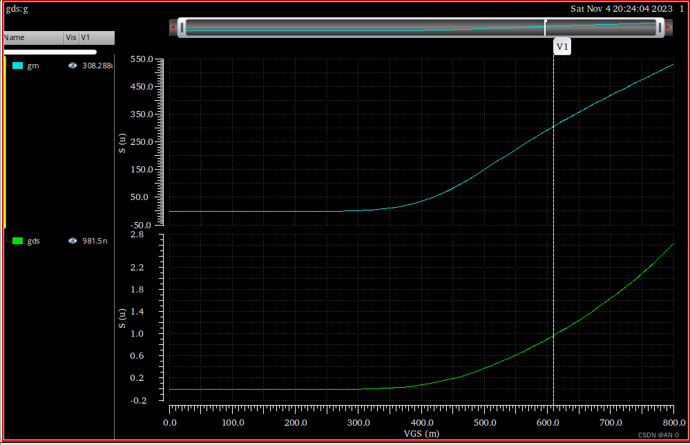
- The remaining variable in the design is to calculate 𝑊. Since the square-law is not accurate, we cannot use it to determine the sizing. Instead, we will use a sizing chart generated from simulation. Create a testbench for NMOS and PMOS characterization (we will use the PMOS later in Part 2 of this lab). Use 𝑊 = 10𝜇𝑚 (we will understand why shortly) and 𝐿 = 2𝜇𝑚 (the same 𝐿 that we chose before).

- Sweep VGS from 0 to ≈ 𝑉𝑇𝐻 + 0.4𝑉 with 10mV step. Set 𝑉𝐷𝑆 = 𝑉𝐷𝐷/2.

- We want to compare 𝑉∗ = 2𝐼𝐷/𝑔𝑚 and 𝑉𝑜𝑣 = 𝑉𝐺𝑆 − 𝑉𝑇𝐻 by plotting them overlaid. Use the calculator to create expressions for 𝑉∗ and 𝑉𝑜𝑣. Export the expressions to adexl.

- Plot 𝑉∗ and 𝑉𝑜𝑣 overlaid vs VGS. Make sure the y-axis of both curves has the same range. You will notice that at the beginning of the strong inversion region, 𝑉∗ and 𝑉𝑜𝑣 are relatively close to each other (i.e., square-law is relatively valid). For deep strong inversion (large 𝑉𝑜𝑣: velocity saturation and
mobility degradation) or weak inversion (near-threshold and subthreshold operation) the behavior is quite far from the square-law (although we are using 𝐿 = 2𝜇𝑚).

- On the 𝑉∗ and 𝑉𝑜𝑣 chart locate the point at which 𝑉∗ = 𝑉𝑄∗. Find the corresponding 𝑉𝑜𝑣𝑄 and 𝑉𝐺𝑆𝑄.

| W | ID |
|---|---|
| 10um | 36.04uA |
| 27.7um | 100uA |
13.Now we are almost done with the design of the amplifier. Note that 𝑔𝑚 is also proportional to 𝑊 as long as 𝑉𝑜𝑣 is constant. On the other hand, 𝑟𝑜 = 1/𝑔𝑑𝑠 is inversely proportional to 𝑊 (𝐼𝐷) as long as 𝐿 is constant. Before leaving this part, calculate 𝑔𝑚𝑄 and 𝑔𝑑𝑠𝑄 using ratio and proportion (crossmultiplication) and double check that 𝐴𝑣 = −𝑔𝑚(𝑅𝐷||𝑟𝑜) meet the required gain spec.
| W | 𝑔𝑚𝑄 |
|---|---|
| 10um | 308.288u |
| 27.7um | 893.957u |
| W | 𝑔𝑑𝑠𝑄 |
|---|---|
| 10um | 981.5n |
| 27.7um | 2718.755n |
Part2 CS Amplifier
- OP and AC Analysis
-
Create a testbench for the resistive loaded CS amplifier using the 𝑉𝐺𝑆𝑄, 𝑅𝐷, 𝐿, and 𝑊 that you got from the previous part.

-
Simulate the DC OP. Report a snapshot for the key operating point (OP) parameters. Compare the results with the results you obtained in Part 1. Since we used chart-based design, the results should agree well


-
Compare 𝑟𝑜 and 𝑅𝐷. Is the assumption of ignoring 𝑟𝑜 justified in this case? Do you expect the error to remain the same if we use min 𝐿?
Answer: Yes, ro=365.33K, RD=9K. So (ro // RD) is close to RD.
No, ro is proportional to L. When L become small the ro will not large enough to ignore it. -
Calculate the intrinsic gain of the transistor.
Answer: Intrinsic Gain = gm x ro = 313.712 -
Calculate the amplifier gain analytically. What is the relation (≪, <, ≈, >, ≫) between the amplifier gain and the intrinsic gain?
Answer: amplifier Gain = gm x RD ≈ 7.72 << Intrinsic Gain. -
Create a new simulation configuration and run AC analysis (from 1Hz to 1GHz). Report the gain vs frequency. Annotate the DC gain and make sure it meets the spec.

the DC Gain is 17.53dB and ie meets the spec.
2.Gain Non-Linearity
-
Create a new simulation configuration. Perform a DC sweep for the input voltage from 0 to 𝑉𝐷𝐷 with 2mV step.

-
Report VOUT vs VIN. Is the relation linear?
Answer: NO. -
Calculate the derivative of VOUT using calculator. Plot the derivative vs VIN. The derivative is itself the small signal gain. Is the gain linear (independent of the input)?

-
Set the properties of the voltage source to apply a transient stimulus (sine wave of 1kHz frequency and 10mV amplitude superimposed on the DC input voltage).

-
Create a new simulation configuration. Run transient simulation for 2ms. Plot gm vs time. Does gm vary with the input signal? What does that mean?

Answer: The gm varies with the input signal. The Gain varies with the input signal, too. It‘ s what we don’t to meet. -
Is this amplifier linear? Comment.
Answer: The Gain varies with the input signal. varies with the VGS.
- Maximum Gain
- We want to investigate the variation of gain vs RD. We will use AC analysis to calculate the small signal gain. Set the source AC magnitude = 1. Note that AC analysis is a linear analysis, so we use a magnitude of one such that the output is itself the gain. Keep the DC value of VGS constant at the DC value you selected in Part 1.
- Set AC simulation to sweep design variable (RD from ¼ the value you selected in Part 1 to 4 times the value you selected in Part 1). Set the AC simulation frequency at 1 Hz (single frequency point). The purpose of the AC analysis here is just to get the small signal gain and not to investigate the frequency response.
- Use the calculator to plot the gain vs RD.

- You will find that the gain increases with RD and then decreases with RD. Justify this behavior.
From 2.25K to 12.375K the gain increases with RD and from 15.75K to 36K decreases with RD. - What is the value of RD that gives the highest gain? What is the highest gain?

Answer: VD=570.008mV and VGS-Vth=610mV - 400mV = 210mV , the available signal swing at the point of maximum gain is from 210mV to 930mV.
- Is scaling down the supply voltage good for gain? Comment.

- Gain Linearization (feedback)
-
We will use feedback to improve the gain non-linearity. We will study feedback in more details later.
-
Create a new schematic and copy the old schematic into it.
-
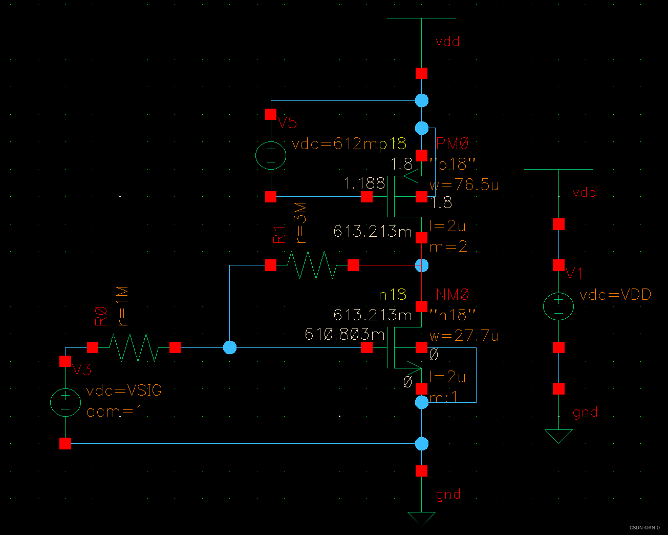
Replace the resistive load with a PMOS current source (active load) as shown below. Create a sizing chart for the PMOS similar to what we did for NMOS in Part 1 using 𝐿 = 2𝜇𝑚 and 𝑊 = 10𝜇𝑚 (you may use the same test bench used in Part 1). From the chart, assuming 𝑉𝑄∗ similar to NMOS, determine 𝑉𝐺𝑆𝑄 and 𝐼𝐷𝑋. Using ratio and proportion (cross-multiplication) determine 𝑊 similar to Part 1. Note that the PMOS load must have the same bias current as the NMOS input device.
-
Note that it is better to bias the PMOS using a voltage source between the gate of the PMOS and VDD.


-
Add two resistors: input resistor (𝑅𝑖𝑛) = 1M and feedback resistor (𝑅𝑓). Choose 𝑅𝑓 to give a voltage gain approximately equal to 𝑅𝑓/𝑅𝑖𝑛 = |𝐴𝑣| as given in the specs.
-
Perform a DC sweep for the input voltage (VSIG) from 0 to 𝑉𝐷𝐷 with 2mV step.
-
Report VIN and VOUT vs VSIG (overlaid). At what voltage do the two curves cross? Why?

-
Is VOUT vs VSIG linear? Why?
Answer: Yes. The gm also does not vary with the time.


 被折叠的 条评论
为什么被折叠?
被折叠的 条评论
为什么被折叠?
 到【灌水乐园】发言


