


1. Functional Description
8-Bit Shift Register/Latch (3-state)
2. General
The 74HC595D is a high speed 8-BIT SHIFT REGISTER/LATCH fabricated with silicon gate C
2
MOS technology.
It achieve the high speed operation similar to equivalent LSTTL while maintaining the CMOS low power dissipation.
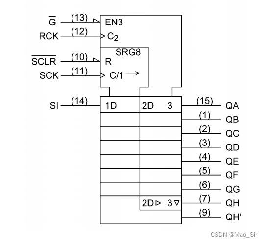
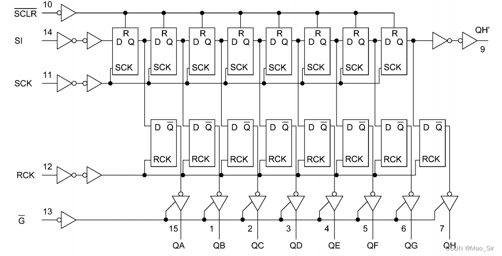
The 74HC595D contains an 8-bit static shift register which feeds an 8-bit storage register.
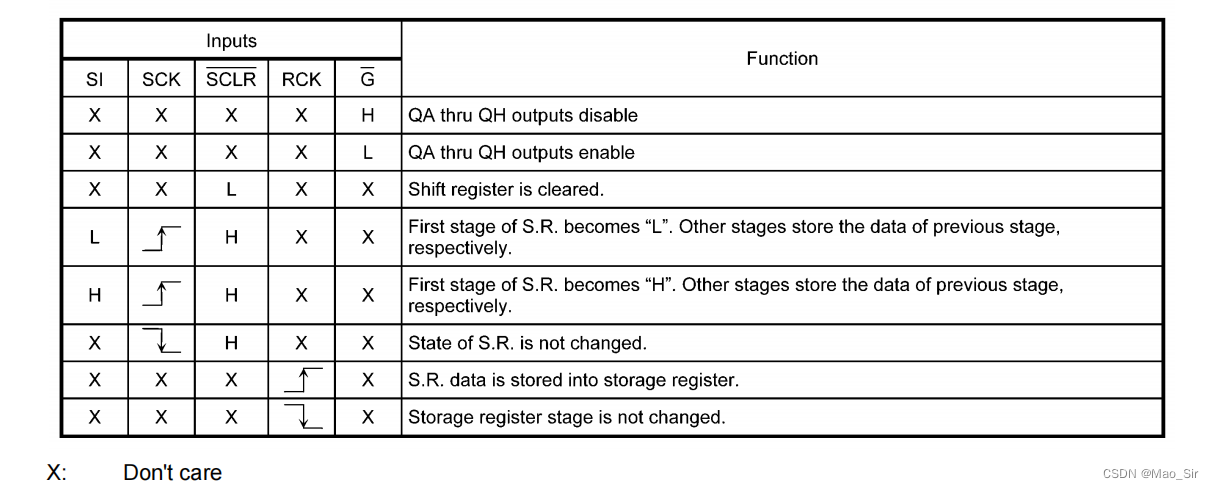
Shift operation is accomplished on the positive going transition of the SCK input. The output register is loaded with the contents of the shift register on the positive going transition of the RCK input. Since RCK and SCK signal are independent, parallel outputs can be held stable during the shift operation.
And, since the parallel outputs are 3-state, it can be directly connected to 8-bit bus. This register can be used in serial-to-parallel conversion, data receivers, etc.
All inputs are equipped with protection circuits against static discharge or transient excess voltage.
3. Features
(1)
High speed: f
MAX
= 55 MHz (typ.) at V
CC
= 5 V
(2)
Low power dissipation: I
CC
= 4.0
µ
A (max) at T
a
= 25°C
(3)
Balanced propagation delays: t
PLH
≈
t
PHL
(4)
Wide operating voltage range: V
CC(opr)
= 2.0 V to 6.0 V
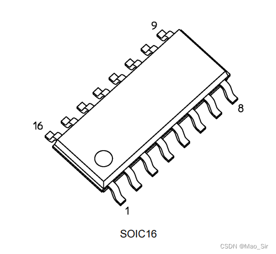
4. Packaging
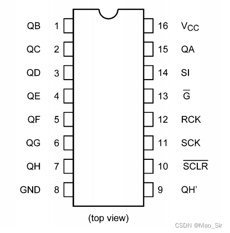
5. Pin Assignment
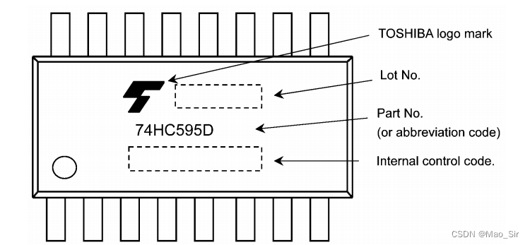
6. Marking
7. IEC Logic Symbol
8. Truth Table
9.Timing Chart

10.System Diagram
11.Absolute Maximum Ratings (Note)
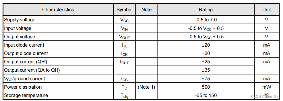
Note:
Exceeding any of the absolute maximum ratings, even briefly, lead to deterioration in IC performance or even destruction.
Using continuously under heavy loads (e.g. the application of high temperature/current/voltage and the significant change in temperature, etc.) may cause this product to decrease in the reliability significantly even if the operating conditions (i.e. operating temperature/current/voltage, etc.) are within the absolute maximum ratings and the operating ranges.
Please design the appropriate reliability upon reviewing the Toshiba Semiconductor Reliability Handbook (“Handling Precautions”/“Derating Concept and Methods”) and individual reliability data (i.e. reliability test report and estimated failure rate, etc).
Note 1:
P
D
derates linearly with -8 mW/°c
above 85 °c
12.Operating Ranges (Note)
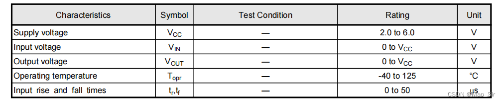
Note:
The operating ranges must be maintained to ensure the normal operation of the device.
Unused inputs must be tied to either V
CC
or GND.
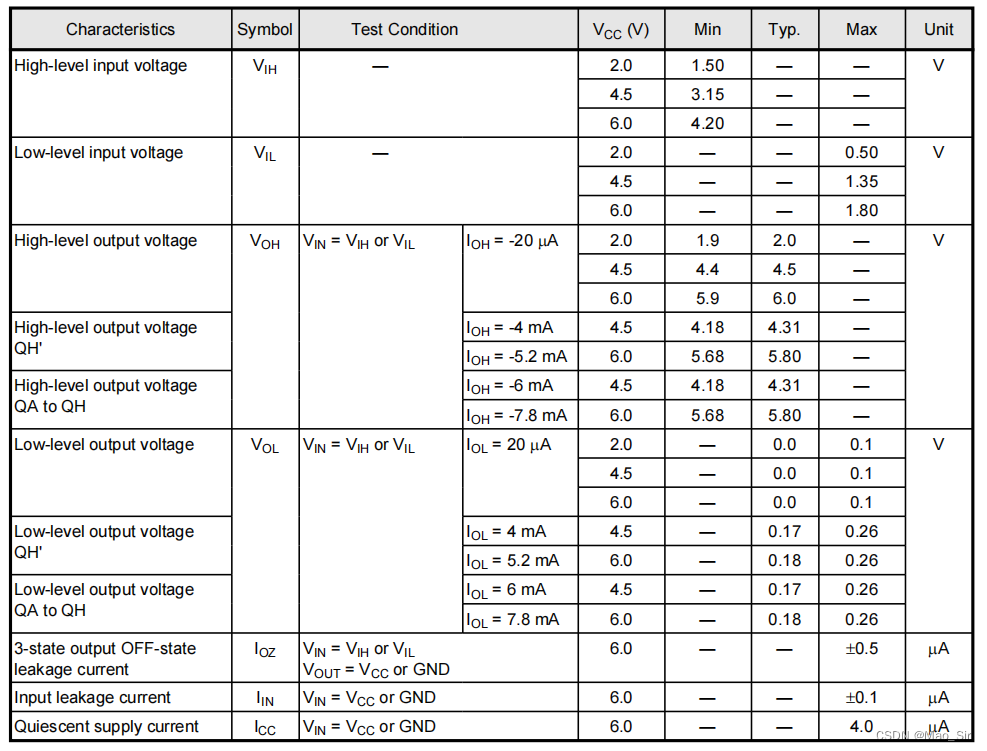
13. Electrical Characteristics
DC Characteristics (Unless otherwise specified, Ta= 25°C


 被折叠的 条评论
为什么被折叠?
被折叠的 条评论
为什么被折叠?
 到【灌水乐园】发言


