


Understanding the HIP programming model#
The HIP programming model makes it easy to map data-parallel C/C++ algorithms to massively parallel, wide single instruction, multiple data (SIMD) architectures, such as GPUs. A basic understanding of the underlying device architecture helps you make efficient use of HIP and general purpose graphics processing unit (GPGPU) programming in general.
RDNA & CDNA Architecture Summary
Most GPU architectures, like RDNA and CDNA, have a hierarchical structure. The innermost piece is a SIMD-enabled vector Arithmetic Logical Unit (ALU). In addition to the vector ALUs, most recent GPUs also house matrix ALUs for accelerating algorithms involving matrix multiply-accumulate operations. AMD GPUs also contain scalar ALUs, that can be used to reduce the load on the vector ALU by performing operations which are uniform for all threads of a warp.
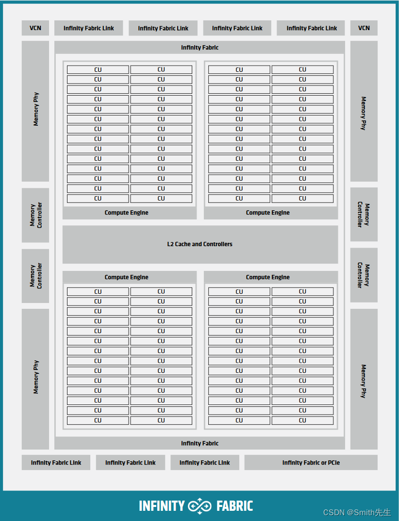
A set of ALUs, together with register files, caches and shared memory, comprise a larger block, often referred to as a compute unit (CU), e.g. in OpenCL and AMD block diagrams, or as streaming multiprocessor (SM).
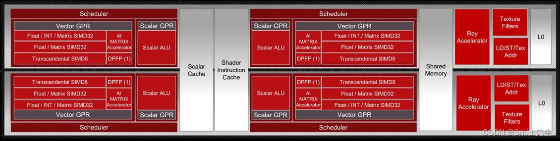
Fig. 1 Block Diagram of an RDNA3 Compute Unit.#

Fig. 2 Block Diagram of a CDNA3 Compute Unit.#
For implementation in hardware, multiple CUs are grouped together into a Shader Engine or Compute Engine, typically sharing some fixed function units or memory subsystem resources.
Heterogeneous Programming
The HIP programming model assumes two execution contexts. One is referred to as host while compute kernels execute on a device. These contexts have different capabilities, therefor slightly different rules apply. The host execution is defined by the C++ abstract machine, while device execution follows the HIP model, primarily defined by SIMT. These execution contexts in code are signified by the __host__ and __device__ decorators. There are a few key differences between the two:
-
The C++ abstract machine assumes a unified memory address space, meaning that one can always access any given address in memory (assuming the absence of data races). HIP however introduces several memory namespaces, an address from one means nothing in another. Moreover, not all address spaces are accessible from all contexts.
If one were to look at Block Diagram of a CDNA2 Graphics Compute Die. and inside the Block Diagram of a CDNA3 Compute Unit., every Compute Unit has an instance of storage backing the namespace
__shared__. Even if the host were to have access to these regions of memory, the performance benefits of the segmented memory subsystem are supported by the inability of asynchronous access from the host. -
Not all C++ language features map cleanly to typical device architectures, some are very expensive (meaning slow) to implement on GPU devices, therefor they are forbidden in device contexts to avoid users tapping into features that unexpectedly decimate their program’s performance. Offload devices targeted by HIP aren’t general purpose devices, at least not in the sense a CPU is. HIP focuses on data parallel computations and as such caters to throughput optimized architectures, such as GPUs or accelerators derived from GPU architectures.
-
Asynchrony is at the forefront of the HIP API. Computations launched on the device execute asynchronously with respect to the host, and it is the user’s responsibility to synchronize their data dispatch/fetch with computations on the device. HIP does perform implicit synchronization on occasions, more advanced than other APIs such as OpenCL or SYCL, in which the responsibility of synchronization mostly depends on the user.
Compute Units#
The basic building block of a GPU is a compute unit (CU), also known as streaming multiprocessor (SM) on NVIDIA GPUs. The thread blocks making up a grid are scheduled for execution on CUs. Each block is assigned to an individual CU, and a CU can accommodate several blocks. Depending on their resource usage up to thousands of threads can reside on a CU.
CUs contain an array of processing elements, referred to as vector ALU (VALU), that execute the actual instructions of the threads according to the SIMT model, together with the necessary registers and caches.
The threads are executed in groupings called warps. The amount of threads making up a warp is architecture dependent. On AMD GPUs the warp size is commonly 64 threads, except in RDNA architectures which can utilize a warp size of 32 or 64 respectively. The warp size of supported AMD GPUs is listed in the Accelerator and GPU hardware specifications. NVIDIA GPUs have a warp size of 32.
In contrast to CPUs, GPUs generally do not employ complex cache structures or control logic, like branch prediction or out-of-order execution, but instead rely on massive hardware multithreading to hide latency.
Context switching between warps residing on a CU incurs no overhead, as the context for the warps is stored on the CU and does not need to be fetched from memory. If there are not enough free registers to accommodate all warps of a block, the block can not be scheduled to that CU and it has to wait until other blocks finish execution.
The amount of warps that can reside concurrently on a CU, known as occupancy, is determined by the warp’s resource usage of registers and shared memory.
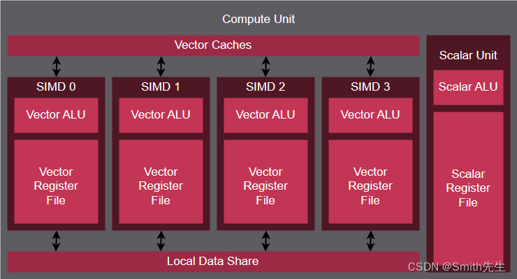
Fig. 8 An AMD Graphics Core Next (GCN) CU. The CDNA and RDNA CUs are based on variations of the GCN CU.
On AMD GCN GPUs the basic structure of a CU is:
-
four Single Instruction Multiple Data units (SIMDs)
-
a vector cache
-
a local data share
-
and a scalar unit
-
SIMD
A SIMD consists of a VALU, that executes the instruction of a warp, together with a register file, that provides the registers warps.
The size of the warp is inherently related to the width of the vector ALU of the SIMD. On GCN compute units the width of the VALU is 16, so a warp can be issued to a SIMD every 4 cycles. Since a CU has 4 SIMDs it issues one warp per cycle. The instructions of a warp are effectively executed in lock-step.
A SIMD always executes the same instruction for the whole VALU. If the control flow of a warp diverges, the performance is decreased, as the results for the threads that do not participate in that branch have to be masked out, and the instructions of the other branch have to be executed in the same way. The best performance can therefore be achieved when thread divergence is kept to a warp level, i.e. when all threads in a warp take the same execution path.
Vector Cache
The usage of cache on a GPU differs from that on a CPU, as there is less cache available per thread. Its main purpose is to coalesce memory accesses of the warps in order to reduce the amount of accesses to device memory, and make that memory available for other warps that currently reside on the compute unit, that also need to load those values.
Local Data Share
The local data share is memory that is accessible to all threads within a block. Its latency and bandwidth is comparable to that of the vector cache. It can be used to share memory between the threads in a block, or as a software managed cache.
Scalar Unit
The scalar unit performs instructions that are uniform within a warp. It thereby improves efficiency and reduces the pressure on the vector ALUs and the vector register file.


 被折叠的 条评论
为什么被折叠?
被折叠的 条评论
为什么被折叠?
 到【灌水乐园】发言


