


 本文深入探讨了ARM处理器的Cache工作原理,包括Cache的作用、类型、组织结构和操作方式。介绍了Cache行、有效位、脏位的概念,并讨论了Cache与主存一致性的问题。文章还提到了启用和禁用Cache的注意事项,以及在多任务环境下MMU如何配合Cache工作,确保内存的正确映射和管理。最后,强调了在任务切换时清理和刷新Cache的重要性。
分享一下我老师大神的人工智能教程!零基础,通俗易懂!http://blog.csdn.net/jiangjunshow
也欢迎大家转载本篇文章。分享知识,造福人民,实现我们中华民族伟大复兴!
cache是ARM最难理解,也是最具有闪光点的地方之一,现在是解决他的时候了。
对于这么经典的东西,我还是引用ARM工程师的书籍吧,免得误人子弟。
cache以及write buffer的介绍
A cache is a small, fast array of memory placed between the processor core and main
memory that stores portions of recently referenced main memory. The processor uses
cachememory instead ofmainmemory whenever possible to increase systemperformance.
The goal of a cache is to reduce the memory access bottleneck imposed on the processor
core by slow memory.
Often used with a cache is a write buffer—a very small first-in-first-out (FIFO) memory
placed between the processor core and main memory. The purpose of a write buffer is to
free the processor core and cache memory from the slow write time associated with writing
to main memory.
cache是否有效以及使能等造成的后果
The basic unit of storage in a cache is the cache line. A cache line is said to be valid when it contains cached
data or instructions, and invalid when it does not. All cache lines in a cache are invalidated on reset. A cache
line becomes valid when data or instructions are loaded into it from memory.
When a cache line is valid, it contains up-to-date values for a block of consecutive main memory locations.
The length of a cache line is always a power of two, and is typically in the range of 16 to 64 bytes. If the
cache line length is 2L bytes, the block of main memory locations is always 2L-byte aligned. Because of this
alignment requirement, virtual address bits[31:L] are identical for all bytes in a cache line
cache所在的位置
——————————————————————————————————————————
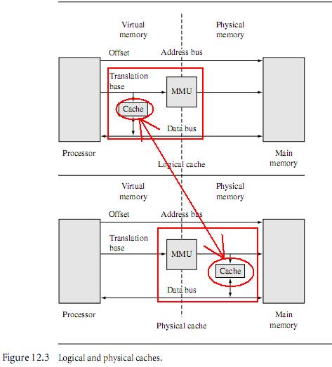
由此可知,cache是可以选择不同位置的,分为物理和虚拟/逻辑类型,但是对于2440是逻辑cache的,请看下图
++++++++++++++++++++++++++++++++++++++==========================================+++++++++++++++++
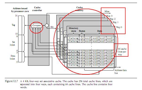
多路cache(单一cache效率很低,不做介绍)
____________________________________________________________________________________________
Tag对应内存中数据的位置,status有两位,一位是有效位(表示所在cache行是否有激活),另外一位
是脏位(判断cache中的内容和内存中的内容是否一致:注意不一致一定要想办法一致,否则后患无穷)
===================================================================================
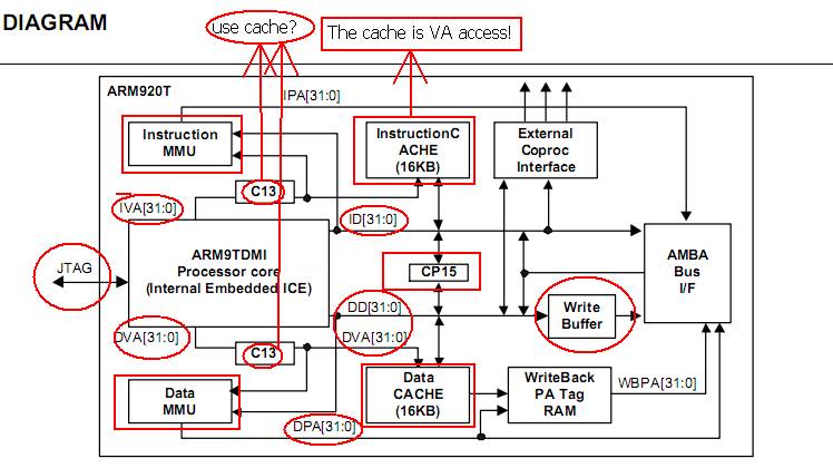
现在来看看和2440靠谱的文档吧(ARM920T)
=====ICache=====
The ARM920T includes a 16KB ICache. The ICache has 512 lines of 32 bytes (8 words),arranged as a 64-way set-associative cache and uses MVAs, translated by CP15 register 13 (see Address translation on page 3-6), from the ARM9TDMI core.The ICache implements allocate-on-read-miss. Random or round-robin replacement can be selected under software control using the RR bit (CP15 register 1, bit 14). Random replacement is selected at reset.Instructions can also be locked in the ICache so that they cannot be overwritten by a linefill.This operates with a granularity of 1/64th of the cache, which is 64 words (256 bytes).All instruction accesses are subject to MMU permission and translation checks. Instruction fetches that are aborted by the MMU do not cause linefills or instruction fetches to appear on the AMBA ASB interface.
Note
————————————————————
For clarity, the I bit (bit 12 in CP15 register 1) is called the Icr bit throughout the
following text. The C bit from the MMU translation table descriptor corresponding to
the address being accessed is called the Ctt bit.
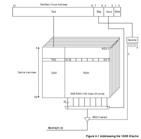
ICache organization(ICache 操作)
——————————————————————————————————————————————————
The ICache is organized as eight segments, each containing 64 lines, and each line
containing eight words. The position of the line within the segment is a number from 0
to 63. This is called the index. A line in the cache can be uniquely identified by its
segment and index. The index is independent of the MVA. The segment is selected by
bits [7:5] of the MVA.
————————————————
Bits [4:2] of the MVA specify the word within a cache line that is accessed. For
halfword operations, bit [1] of the MVA specifies the halfword that is accessed within
the word. For byte operations, bits [1:0] specify the byte within the word that is
accessed.
—————————————————
Bits [31:8] of the MVA of each cache line are called the TAG. The MVA TAG is store
in the cache, along with the 8-words of data, when the line is loaded by a linefill.——所有cache的读写原理都是一样的
—————————————————
Cache lookups compare bits [31:8] of the MVA of the access with the stored TAG to
determine whether the access is a hit or miss. The cache is therefore said to be virtually
addressed. The logical model of the 16KB ICache is shown in Figure 4-1 on page 4-5.
++++++++++++++++++++++++++++++++++++++++++++++++++++++++++++++++++++++++++++++++++++++++++++++
Enabling and disabling the ICache
————————————————
On reset, the ICache entries are all invalidated and the ICache is disabled.
You can enable the ICache by writing 1 to the Icr bit, and disable it by writing 0 to the
Icr bit.
When the ICache is disabled, the cache contents are ignored and all instruction fetches
appear on the AMBA ASB interface as separate nonsequential accesses. The ICache is
usually used with the MMU enabled. In this case the Ctt in the relevant MMU
translation table descriptor indicates whether an area of memory is cachable.
If the cache is disabled after having been enabled, all cache contents are ignored. All
instruction fetches appear on the AMBA ASB interface as separate nonsequential
accesses and the cache is not updated. If the cache is subsequently re-enabled its
contents are unchanged. If the contents are no longer coherent with main memory, you
must invalidate the ICache before you re-enable it (see Register 7, cache operations
register on page2-17).——主存和cache的内容不一致,在重新使能ICache之前必须清除ICache
————————————————————————————————————
If the cache is enabled with the MMU disabled, all instruction fetches are treated as
cachable. No protection checks are made, and the physical address is flat-mapped(?) to the
modified virtual address.(使能cache,但是禁用MMU,指令存取是cachable的,没有保护检查
物理地址等于虚拟地址。)
You can enable the MMU and ICache simultaneously(同时地) by writing a 1 to the M bit, a
1 to the Icr bit in CP15 register 1, with a single MCR instruction.
————————————————————————————————————
If the ICache is disabled, each instruction fetch results in a separate nonsequential
memory access on the AMBA ASB interface, giving very low bus and memory
performance. Therefore, you must enable the ICache as soon as possible after reset.
————————————————————————————————————
Note
The Prefetch ICache Line operation uses MVA format, because address aliasing(混淆现象) is not
performed on the address in Rd. It is advisable for the associated TLB entry to be locked
into the TLB to avoid page table walks during execution of the locked code.
————————————————————————————————————
Enabling and disabling the DCache and write buffer
On reset, the DCache entries are invalidated and the DCache is disabled, and the write
buffer contents are discarded(放弃).
——————————————
There is no explicit(直接的,清楚的) write buffer enable bit implemented in
 最低0.47元/天 解锁文章


 1万+
1万+

 被折叠的 条评论
为什么被折叠?
被折叠的 条评论
为什么被折叠?
 到【灌水乐园】发言


