


Wafer microbumping packaging, more commonly expressed as Wafer Microbumping or Wafer Bumping, is an advanced semiconductor packaging technology.The following is a detailed explanation of Wafer Bumping:
I. Definitions and rationale
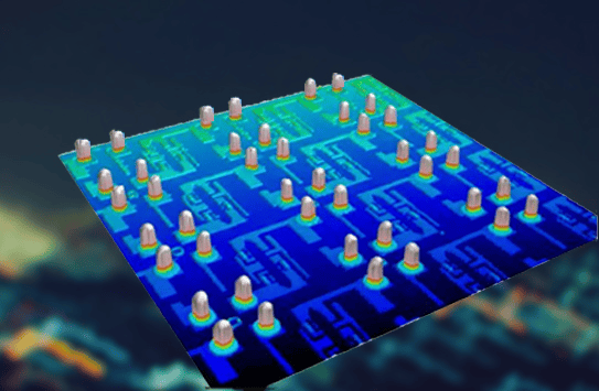
Wafer micro-bump packaging refers to the formation or installation of tiny bumps (also known as bumps) at pre-determined locations on the wafer before it is cut into individual chips, which will serve as interfaces between the chip and external circuitry.The principle involves creating a series of bumps on the surface of the wafer to interconnect the chip to a PCB (printed circuit board) or substrate.
II. Methods of Bump Formation
Wafer bumping technology includes a number of different bump formation methods, such as:
Printed bumps: Bumps are formed on wafers by
 最低0.47元/天 解锁文章


 被折叠的 条评论
为什么被折叠?
被折叠的 条评论
为什么被折叠?
 到【灌水乐园】发言


