


文章目录
- Preface to the Paperback Edition
- Chapter 1 . Best Friends (至亲密友)
- Chapter 2 Codes and Combinations
- Chapter 3 Braille and Binary codes
- Chapter 4 Anatomy of a flashlight
- Chapter 5 Seeing Around Corners
- Chapter 6 Telegraphs and Relays
- Chapter 7 Our Ten Digits
- Chapter 8 Alternatives to Ten
- Chapter 9 Bit by Bit by Bit
- Chapter 10 Logic and Switches
- Chapter 11 Gates (Not Bill)
- Chapter 12 A Binary Adding Machine
- Chapter 13 But What About Subtraction
- Chapter 14 Feedback and Flip-Flops
- Chapter 15
Preface to the Paperback Edition
Chapter 1 . Best Friends (至亲密友)
两个小孩子试图在网上互相交流,
但是电话不可行,因为首先要有电话,然后也容易被偷听到。
然后考虑个人电脑,但是应该有吗?不应该的。
最后,决定采取的方案使手电筒。
方法
- 首先考虑模仿在纸上写字的方式,但是不行,一是灯光不够精准,二是大脑不够发达,无法将手电筒挥舞出来的笔划拼接出来。
- 将手电筒的闪光和字母表中的字母一一对应起来,比如A为1个闪烁,B为2个闪烁。然后在字母之间加上间隔,用来作为标志。
- 然而问题出现了,太长了,即使简单的一句话,都需要很多次灯光的闪烁。
- 那么去寻找前任的经验吧,看看是否能够利用前人的智慧。
- 出现了,是它 是它 就是它, Morse code.
常见的编码有很多,包括语言其实就最常见的一种编码
- spoken word or speech
- the written word or text
- sign language
最后就是发现,数字2 ,两个不同的东西,经过组合可以表示所有类型的信息。
Morse code 的方式:
使用点和划的序列表示不同的含义,比如26个英文字母。一个字母比如A,它的序列中点和划之间要有停顿; 字母与字母之间如A和B,它们之间也需要停顿,并且需要比单个字母中的停顿要长,用于区分。
Chapter 2 Codes and Combinations
Morse code 的接收比发送要难很多。
通过树状图,来检索Morse code 对应的字母
这一章讲了2进制的排列组合,很简单的数学理论。把不同的排列组合分配给不同的字母或者其他字符。
这里比较有意思的感觉还是上面的树状检索。可以很快检索到Morse code对应的字符是什么
Chapter 3 Braille and Binary codes
Chapter 4 Anatomy of a flashlight
- 关于电流的形成,是有于电子的移动
- 原子包含:质子、中字、电子,其中质子带正电,电子带负电,中子不带点
- 异性电荷互相吸引,同性电荷互相排斥。
简单电路的介绍。
- 开关只能是闭合状态和断开状态
- 电流只能是有和无
- 灯泡只能是发光或不发光
- 这都和摩尔斯和布莱叶发明的二进制码一样。
- 这种二进制码和电气电路之间的相似性会有很大的作用。
Chapter 5 Seeing Around Corners
使用电路在你和朋友的房间中分别连接一个灯泡,然后使用灯泡去传递信息是很不错的。
但是有一个问题就是如果长距离的时候,那么由于电阻的问题将导致无法产生足够的电流点亮灯泡,一些如加大电压,增加导线厚度的解决方案会很昂贵,而且不足以解决长距离问题。
Chapter 6 Telegraphs and Relays
Morse使用电磁学原理:充电线圈围在铁棒上,可以使铁棒带有磁性,进而吸引其他的铁棒或者金属,进而达到了在一端闭合或断开开关时,能够在另一端产生一些变化,这样就能够进行信息的传递。(没有使用电灯的亮或灭,是因为那时候没有电灯)。
但是问题在于长导线带来的电阻使得距离仍旧不能无限延伸。
其中一个解决方法是: 中继系统 relay system 。 每隔一定距离,将收到的结果再次转发出去。
自动化: 将进入的电流产生的磁力拉去下来的铁棒作为另一个开关,这样就可以实现自动化,其实也就是中继器。因为近来的时候是弱电流,但是出去的时候又变成了强电流了。而且这个过程不需要人去操作。
Chapter 7 Our Ten Digits
计算方式的出现到阿拉伯数字,一个很伟大的存在,它属于位置相关的计数方式,即数字的大小不仅仅和其本身有关,还和它所在的位置相关,这种方式有利于减法和乘法的运算。
最常见的基于位置的计算方式是十进制,但是其他位数的如8进制,2进制,也同样适用很多性质。
Chapter 8 Alternatives to Ten
8进制的加法和乘法基本规则同于十进制,只不过乘法表和加法表有所变化。
然后进一步发展到4进制,2进制
最后止于2进制的计算和2进制与导线、开关,灯泡,电报继电器等之间的关系,
最后是二进制会与computer 产生密切关系。
Chapter 9 Bit by Bit by Bit
2进制,明确表示yes or no ,可以做很多事情
bit可以表示文字、图片、声音、音乐、电影,也可以表示产品编码、胶片速度、影评结果、英国军队的入侵以及心爱之人的意图。但是从根本上来说,比特是数字。在用比特表示其他信息的时候我们所要做的就是计算有多少种可能性。这决定我们所需要的的比特位数,以便每种可能性都可以分配一个编号。
bit在逻辑学中也很重要。 逻辑学是哲学和数学的奇特融合,其主要目的就是确定某个陈述是真是假。真和假同样可以表示为1和0.
Chapter 10 Logic and Switches
电路和布尔的逻辑代数能够起到一一对应关系。
两个开关串联对应逻辑 and
两个开关并联对应逻辑 or
灯泡的明亮与否代表结果
那么就算没有灯泡,其实也可以使用电报机来代替灯泡实现这个效果啊!!!
那么构建一个计算机的条件是否已经充足了呢?
下面一章根据电报器来创建计算机。
Chapter 11 Gates (Not Bill)
Logic gates perform simple tasks in logic by blocking or letting through the flow of electrical current.
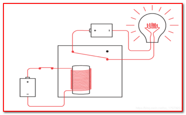
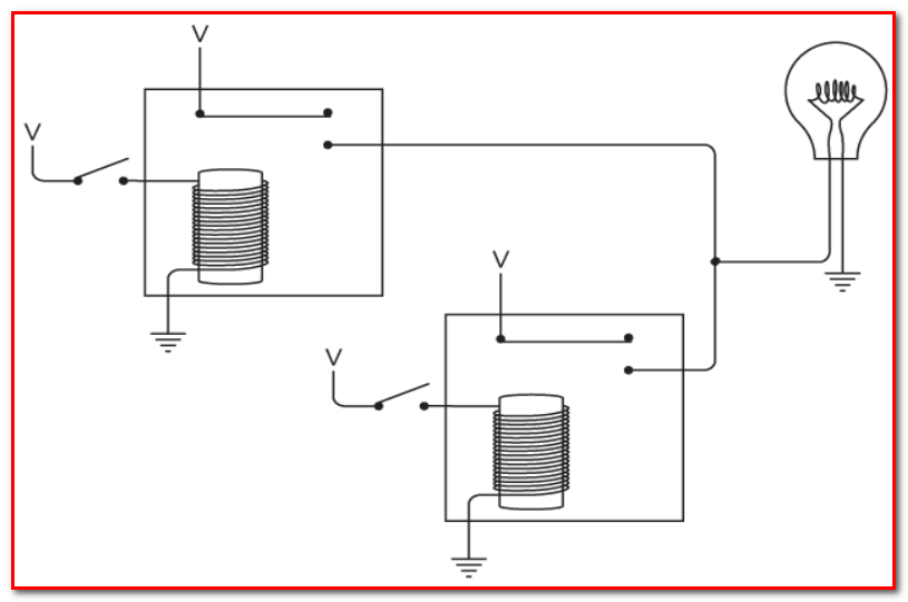
继电器:
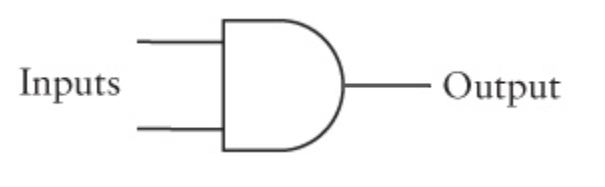
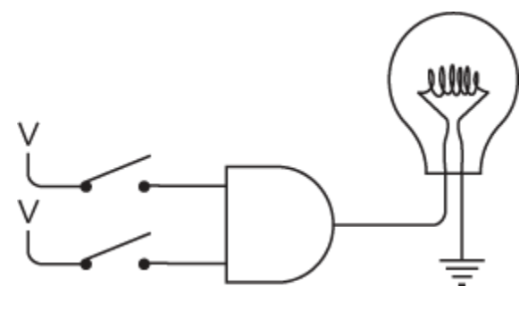
AND gate
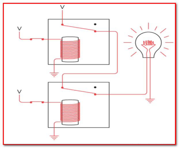
AND
The original circuit with the two relays wired in series with two switches and a lightbulb looked like this :
Using the symbol for the AND gate ,this same circuit looks like this :
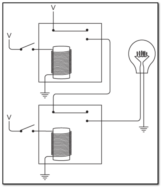
与门的输入不一定要和开关相连,而且输出也不一定只能和灯泡相连。我们真正要处理的是输入端的电压和输出端的电压。
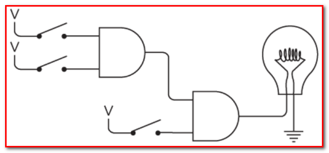
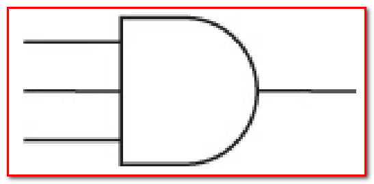
同样可以让与门有多个输入端,例如将三个继电器并联
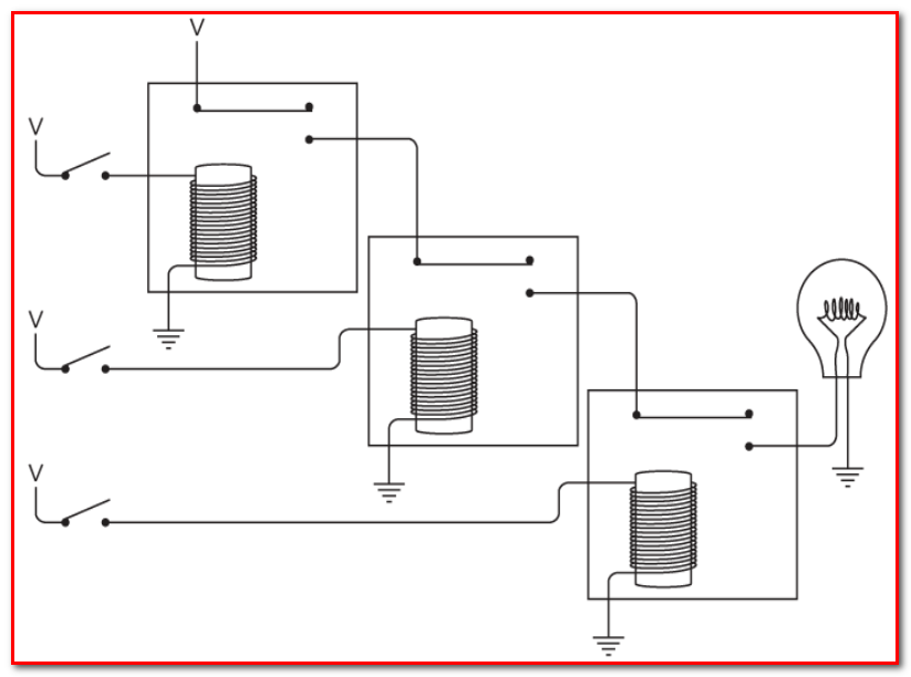
this configuration is expressed by this symbol
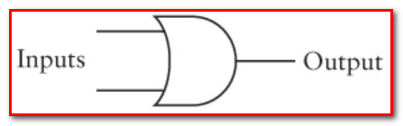
The next logic gate involves two relays that are wired in parallel like this:
OR gate looks like this
inverter : 反相器

继电器 表示 NOT OR

NOT OR (NOR)

The output of the NOR gate is shown in the following table
| NOR | 0 | 1 |
|---|---|---|
| 0 | 1 | 0 |
| 1 | 0 | 0 |
Only when both switches are closed does the lightbulb go off:

The NAND gate is drawn just like the AND gate but with a circle at the output, meaning the output is the inverse of the AND gate .

The NAND gate has the following behavior:
| NAND | 0 | 1 |
|---|---|---|
| 0 | 1 | 1 |
| 1 | 1 | 0 |
四种逻辑门的总结(外加一个inverter )
The output of the particular logic gate depends on the input, which is summarized here

buffer: you can use a buffer when an input signal is weak

buffer

从这里开始,本书就很少有继电器的图片了。
Instead, the circuits that follow will be built from buffers, inverters, the four basic logic gates, and more
sophisticated circuits (like the 2-Line-to-4-Line Decoder) built from these logic gates .
后面反向器有时也会简化

to

An AND gate with two inverted inputs does exactly the same thing as a NOR gate:

Similarly, an OR gate with the two inputs inverted is equivalent to a NAND gate:

De Morgan’s Laws are most simply expressed this way:

And what we’re going to get working next is nothing less than an adding machine
下一章开始加法器
Chapter 12 A Binary Adding Machine
二进制加法器的实现
通过前面学到的内容:switches, lightbulbs, wires, a battery, and relays
和现代计算机相比:没有键盘输入和屏幕输出,对应的是开关输入和灯泡输出,但是注重点在原理,原理,原理!
- You won’t be able to use a keyboard to indicate the numbers you want to add; instead you’ll use a row of switches.
- Rather than a numeric display to show the results, this adding machine will have a row of lightbulbs
我们的加法器大概是这个样子:上面两排开关是输入设备可以输入两个8位二进制数,下面的一排灯泡就是结果。
The control panel for our binary adding machine can look like this:
- This collection of switches is the input device, and we’ll use it to “key in” the two 8-bit numbers.
- The output device at the bottom of the panel is a row of nine lightbulbs .These bulbs
will indicate the answer

The switches will trigger the relays in the logic gates
这些开关会触发继电器(在逻辑门中的),然后使下面的灯正确的亮起来。
下面是一个例子:要进行相加的两个数字和对应的面板


加法的计算分为bit和,和bit进位:
the first one for the sum bit

and the second one for the carry bit:

首先实现进位:会发现进位和AND逻辑门是一样的,那么很好就是用AND门进行进位的计算
然后开始计算the sum bit
The first thing to realize is that the OR gate is close to what we want except for the case in the lower right corner:

The NAND gate is also close to what we want except for the case in the upper left corner:

So let’s connect both an OR gate and a NAND gate to the same inputs:
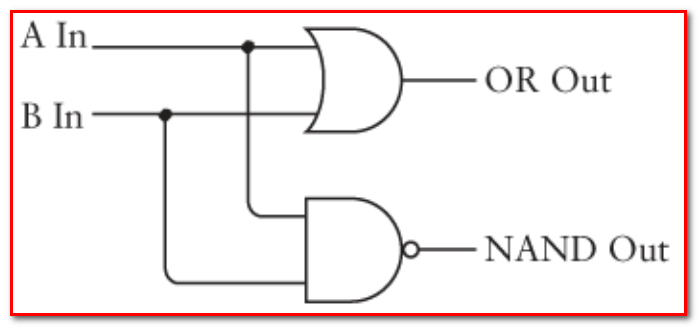
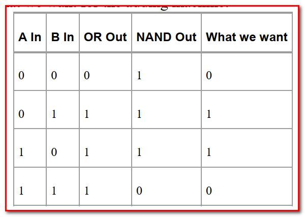
The following table summarizes the outputs of these OR and NAND gates and compares that to what we want for the adding machine:
如果忽略中间过程(当然我没有忽略),那么最后逻辑图为:
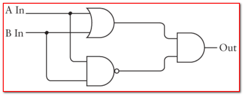
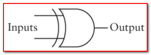
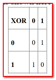
上面这个电路图其实还有一个名字,那就是异或门 :the XOR gate.
It’s called the Exclusive OR gate because the output is 1 if the A input is 1 or the B input is 1, but not both.
下面是对应的电气工程师使用的符号:
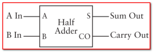
Half Adder
之所以叫半加器,自然有其缺陷:因为它没有考虑到进位。
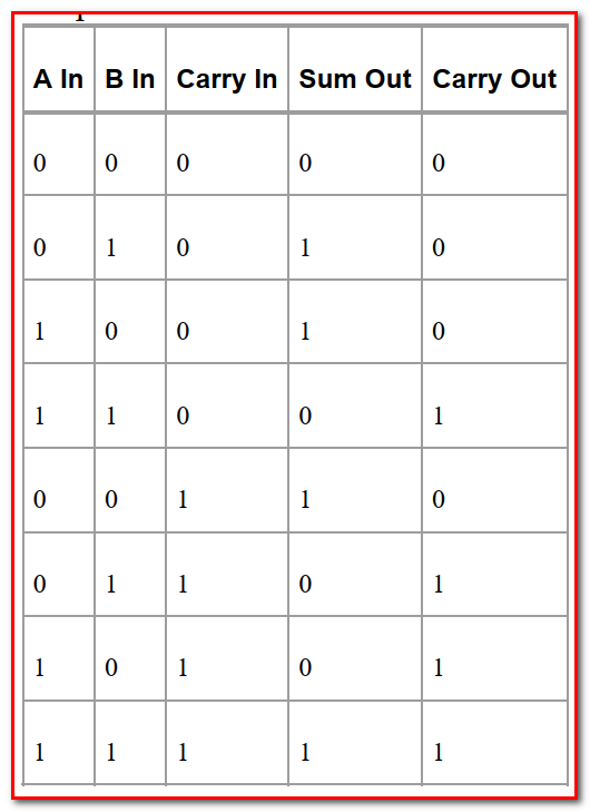
真正的加法器需要进行3个bit的运算
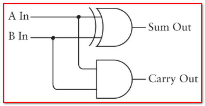
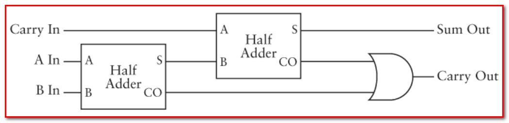
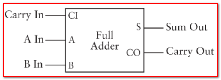
full adder
全加器是有两个半加器和一个OR门组成的。
一个全加器= 两个半加器+OR门= 2(AND门+异或门) + OR门 = 2(AND门 + (2个 AND门+ 1个OR门))+ 1个 OR门 = 6 个AND门 + 3 OR门 = 18 个继电器
Chapter 13 But What About Subtraction
如何实现减法 ?
想想都觉得好麻烦啊,减法中居然有借位的说法,毫无头绪。
首先对涉及到的三个数字进行命名: Minuend 被减数 、 Subtrahend 减数、 difference 差
既然借位搞不定,那么就避开它,不要借位。
看253-176
- 253-176 等价于
- 253-176+1000-1000
- 253-176+999+1-1000
- 253+(999-176)+1 -1000
此时就不会存在借位问题了。
接下来看176-253,此时减数大于被减数。
- 176 - 253
- 176 + (999 - 253) - 999
- -(999 - (176 + (999 - 253)))
这个过程也将借位给规避掉了。
开始进行减法器的构造
减法器

one’s complement is equivalent to inverting bits
eight inverters:

XOR 门: 当invert为0时,输出为原本的输入;当invert为1时,输出为输入的相反


Let’s package these eight XOR gates in a box labeled Ones’ Complement:

The Ones’ Complement box, the 8-Bit Adder box, and a final exclusive OR gate can
now be wired together like this:
下面这个图的说明:
- 如果是减法,则B的输入先变为 one’s implement 也就是全部相反。
- CI (carry in )为1
- 如果是加法,则B的输入不变化,且CI 为0
- 当sub为0,为加法;当sub为1,为减法
- 当加法时,如果A+B>255 时, CO为1,sub为0,此时overflow
- 当减法时,如果A>B时,sub为1,CO为1,此时为指示灯不亮。如果A<B,此时,此时A+B的one’s complement < 1 0000 0000 ,此时为负数,这个器件不能表示负数。
注意上面过程的减法中其实只做加法操作:A + B的inverter,然后溢出代表的就是那个减去的1 0000 0000 ;所以它没办法表示A < B ,因为如果A < B ,按照 A + B的invert + 1 - 1 0000 0000 这种方式就不准了。此时应该是 -(1111 1111 - (A + B 的invert)),下面这个没有这个功能。

来一部分二进制补码的规律:
正数取反+1 为对应的负数;
负数取反+1 为对应的正数。
- 1011 0110 (-74的补码形式)
- 0100 1001 (取反)
- 0100 1010 (+1)
- 计算为:2+8+64 = 74
在来一个例子
- 0100 1010 (74的补码形式,就是其本身)
- 1011 0101 (取反)
- 1011 0110 (+1,就是-74的补码形式)
所以想要知道一个负数补码形式对应的十进制的值,先得到对应的正数,然后就知道这个负数是多少了。
最后减法器是否完全实现了呢,其实还没有,我补充一下:
首先计算机内部二进制全部使用补码形式,然后直接进行加法运算即可。
Chapter 14 Feedback and Flip-Flops
继电器、电池、开关这样组合

振荡器
振荡器只要最初的开关已闭合,就会不断地输出与输入相反的信号,然后将输出再次作为输入。

also :

振荡器的作用是自动化。
我怀疑时钟是不是就是根据振荡器搞得?(果然是时钟,后面的文章提到了)
振荡器的表示:

振荡器周期

feedback:

feedback : 反馈
flip-flops : 触发器
触发器的作用: 具有记忆功能。
R-S (or Reset-Set) flip-flop | R-S触发器


R-S 触发器: 能够记住是哪个输出端最后保持电压。
例如当S和R都为0时,如果你将S闭合,此时S变为1,然后观察Q是否变化,如果没有变化,则证明最后闭合的是S,否则最后闭合的是R。
What turns out to be much more useful, however, is a circuit that remembers whether a particular signal was 0 or 1 at a
particular point in time.
我们更需要及时知道在某个点的一个信号是0还是1.
接下来看看如何实现这个触发器把。
level-triggered D-type flip-flop
the flip-flop saves the value of the Data input when the Hold That Bit input is at a particular level, in this case 1
当clock为1时,data的值会被保存在触发器的输出中,当clock 为0 时,data的任何变化都不会影响到触发器的输出(还保持原状)。


就上面这玩意,许多个这样的触发器,可以构成多位存储器… 厉害了。
edge-triggered Clock 边缘触发时钟
在边沿触发器中,只有在时钟输入从0变1的瞬间,数据端的输入才会影响边沿触发器的输出。
电路图

1 初始态

2 Data :0到1
结果:输入Q不变化

Clock: 0-1
结果: 输出的Q为Data的值
[外链图片转存失败,源站可能有防盗链机制,建议将图片保存下来直接上传(img-ogmWFgcf-1598288222712)(https://i.loli.net/2020/08/25/IfLDuGT5h1BVdae.png)]
使用向上的箭头表示0到1的瞬间变化

触发器的符号表示

Chapter 15
文章目录
- Preface to the Paperback Edition
- Chapter 1 . Best Friends (至亲密友)
- Chapter 2 Codes and Combinations
- Chapter 3 Braille and Binary codes
- Chapter 4 Anatomy of a flashlight
- Chapter 5 Seeing Around Corners
- Chapter 6 Telegraphs and Relays
- Chapter 7 Our Ten Digits
- Chapter 8 Alternatives to Ten
- Chapter 9 Bit by Bit by Bit
- Chapter 10 Logic and Switches
- Chapter 11 Gates (Not Bill)
- Chapter 12 A Binary Adding Machine
- Chapter 13 But What About Subtraction
- Chapter 14 Feedback and Flip-Flops
- Chapter 15


 2573
2573

 被折叠的 条评论
为什么被折叠?
被折叠的 条评论
为什么被折叠?
 到【灌水乐园】发言


