


Notes 1, 2 & 14 apply to the entire Command truth table
To improve command decode time, the table has been optimized to orient all 1-cycle commands together and all 2-cycle commands together; allowing CA1 to be used to identify the difference between a 1-cycle and a 2-cycle command. (CA1=L : 2 cycle cmd ; CA1=H : 1cycle cmd)
[ BG=Bank Group Address, BA=Bank Address, R=Row Address, C=Column Address, MRA=Mode Register Address, OP=Op Code, CID=Chip ID, DDPID=Dual Die Package ID, CW=Control Word, X=Don’t Care, V=Valid ]
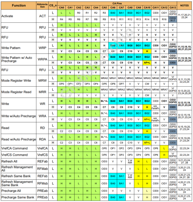

NOTE 1 V means H or L (a defined logic level). X means don't care in which case the signal may be floated.
NOTE 2 Bank group addresses BG[2:0] and Bank addresses BA[1:0] determine which bank is to be operated upon in a specific bank group.
NOTE 3 The Refresh All and Refresh Management All commands are applied to all banks in all bank groups. CA6 and CA7 are required to be valid (“V”)
NOTE 4 The Refresh Same Bank and Refresh Management Same Bank commands refresh the same bank in all bank group bits. The bank bits, BA0 and BA1 on CA6 and CA7, respectively, specify the bank within each bank group.
NOTE 5 The Precharge All command applies to all open banks in all bank groups.
NOTE 6 The Precharge Same Bank command applies to the same bank in all bank groups. The bank bits specify the bank within each bank group.
NOTE 7 The Precharge command applies to a single bank as specified by bank address and bank group bits.
NOTE 8 CS_n=LOW during the 2nd cycle of a two cycle command controls ODT in non-target ranks for WR, RD and MRR commands.
NOTE 9 The SRE command places the DRAM in self refresh state
NOTE 10 The PDE command places the DRAM in power down state
NOTE 11 Two cycle commands with no ODT control (ACT, MRW, WRP). DRAM does not execute the command if it receives CS as LOW on 2nd cycle.
NOTE 12 WR command with WR_partial = Low indicates a partial write command. This is to help DRAM start an internal read for 'read modify write'.
NOTE 13 If CW=Low during the MRW command then DRAM should execute the command, Mode Register will be written. If CW=HIGH then DRAM ignores the MRW command, and the Mode Register is not changed. During MRR commands the DRAM ignores the value of the CW bit, MRR will be executed if CW=Low or CW=High.
NOTE 14 CID[3:0] bits are used for 3DS stacking support.
NOTE 15 If CA5:BL*=L, the command places the DRAM into the alternate Burst mode described by MR0[1:0] instead of the default Burst Length 16 mode.
NOTE 16 ODT=L is defined to allow On Die Termination (ODT) to persist when the device is in Power Down Mode.
NOTE 17 CID3/R17 is a multi-mode pin allowing for either 16H 3DS stacking with the CID3 bit usage or R17 for high bit density monolithic usage. These usages are mutually exclusive.
NOTE 18 Write Pattern only supports BL16 and BL32.
NOTE 19 When CID3 is not used, its CA decode is VALID.
NOTE 20 In the case of a DRAM where the density or stacking doesn't require CA[13] the ball location for that function (considering the state of MIR) shall be connected to VDDQ, and the DRAM shall decode CA[13]=L so that the proper selection of die and RA is provided.
NOTE 21 CID2/DDPID is a multi-mode pin allowing for either 3DS stacking with CID2 or DDP packaging with DDPID. Use of 3DS and DDP are mutually exclusive.
NOTE 22 V/DDPID is a multi-mode pin where the DDPID is used for DDP packages only.
NOTE 23 Any command using DDPID shall issue a NOP to non-selected device.
NOTE 24 NT-ODT behavior is not influenced by DDPIP value
NOTE 25 CA[0:1] =[L:L] on the second cycle for burst ordering.
NOTE 26 When host issue MRR with CRC enabled, data comes out with CRC bit.
NOTE 27 If the Refresh Management Required bit is “0” (MR58 OP[0]=0), CA9 is only required to be valid (“V”).
NOTE 28 If the Refresh Interval Rate indicator bit is disabled (MR4:OP[3]=0), CA8 is only required to be valid (“V”). If the Refresh Interval Rate indicator bit is enabled (MR4:OP[3]=1), the host will set CA8=H for REF commands issued at the 1x refresh interval rate and CA8=L for REF commands issued at the 2x refresh interval rate.


 1065
1065


 被折叠的 条评论
为什么被折叠?
被折叠的 条评论
为什么被折叠?
 到【灌水乐园】发言


