


目录
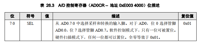
3.1、A/D控制寄存器( AD0CR - 0xE003 4000)
3.2、A/D全局数据寄存器( AD0GDR - 0xE003 4004)
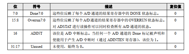
3.3、A/D状态寄存器( ADSTAT - 0xE003 4030)
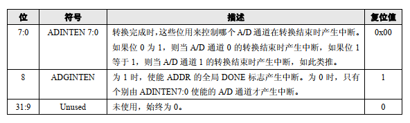
3.4、A/D中断使能寄存器( ADINTEN - 0xE003 400C)
3.5、A/D数据寄存器( ADDR0~ADDR7 - 0xE003 4010~0xE003 402C)
1、开发环境
LPC-2478STK+IAR+JINK
2、原理图
对应的是ADC0[7]-> P0[13],PINSEL0应设置为11

![]()
3、相关寄存器
A/D 转换器的基本时钟由 APB 时钟(PCLK)提供。 每个转换器包含一个可编程的分频器,它可将这个时钟调整为逐次逼近转换所需的 4.5MHz(最大)。完全满足精度要求的转换需要 11 个这样的时钟。
3.1、A/D控制寄存器( AD0CR - 0xE003 4000)

3.2、A/D全局数据寄存器( AD0GDR - 0xE003 4004)

3.3、A/D状态寄存器( ADSTAT - 0xE003 4030)
3.4、A/D中断使能寄存器( ADINTEN - 0xE003 400C)
3.5、A/D数据寄存器( ADDR0~ADDR7 - 0xE003 4010~0xE003 402C)

4、触发方式
如果 ADCR 的 BURST 位为 0 且 START 字段的值包含在 010-111 之内,那么当所选管脚或定时器匹配信号发生跳变时 A/D 转换器启动一次转换。也可选择在 4 个匹配信号中任何一个的指定边沿转换,或者在 2 个捕获/匹配管脚中任何一个的指定边沿转换。将所选端口的管脚状态或所选的匹配信号与 ADCR 的位 27 异或来作为边沿检测逻辑。
5、代码实现
#include <nxp/iolpc2478.h>
#include <intrinsics.h>
typedef unsigned char  u8;
typedef unsigned short u16;
typedef unsigned int  u64;
typedef unsigned long  u32;

#ifndef NULL
#define NULL ((void*)0)
#endif

/* P1[13] 低电平导通 */
#define led1            13
/* P1[18] 低电平导通 */
#define led2            18
/* P2[19] 按下低电平,悬空高电平 */
#define but1            19
/* P2[21] 按下低电平,悬空高电平 */
#define but2            21

#define led1_on         (FIO1CLR |= 0x01 << led1)
#define led1_off        (FIO1SET |= 0x01 << led1)
#define led2_on         (FIO1CLR |= 0x01 << led2)
#define led2_off        (FIO1SET |= 0x01 << led2)

void enable_fast_port()
{
  SCS |= 1 << 0;
}
void gpio_init()
{
  PINSEL2 &= ~(0x03 << led1*2);
  FIO1DIR &= ~(0x01 << led1);
  FIO1DIR |=   0x01 << led1;
  led1_off;
  PINSEL3 &= ~(0x03 << ((led2 % 16)*2));
  FIO1DIR &= ~(0x01 << led2);
  FIO1DIR |=   0x01 << led2;
  led2_off;

  PINSEL5 &= ~(0x03 << ((but1 % 16)*2));
  PINSEL5 |=   (0x0 << ((but1 % 16)*2));
  FIO2DIR &= ~(0x01 << but1);

  PINSEL5 &= ~(0x03 << ((but2 % 16)*2));
  PINSEL5 |=   (0x0 << ((but2 % 16)*2));
  FIO2DIR &= ~(0x01 << but2);
}
void led1_reverse(void)
{
  if ((FIO1SET & (0x01 << led1)) == 0)
    led1_off;
  else
    led1_on;
}

void led2_reverse(void)
{
  if ((FIO1SET & (0x01 << led2)) == 0)
    led2_off;
  else
    led2_on;
}

u32 irq_result;
void adc_irq(void)
{
  irq_result = AD0GDR_bit.RESULT;
  VICADDRESS 	= 0x00;
}
void VIC_SetVectoredIRQ(void(*pIRQSub)(), unsigned int Priority,
                        unsigned int VicIntSource)
{
unsigned long volatile *pReg;
  // load base address of vectored address registers
  pReg = &VICVECTADDR0;
  // Set Address of callback function to corresponding Slot
  *(pReg+VicIntSource) = (unsigned long)pIRQSub;
  // load base address of ctrl registers
  pReg = &VICVECTPRIORITY0;
  // Set source channel and enable the slot
  *(pReg+VicIntSource) = Priority;
  // Clear FIQ select bit
  VICINTSELECT &= ~(1<<VicIntSource);
}
__irq __arm void IRQ_Handler (void)
{
void (*interrupt_function)();
unsigned int vector;

  vector = VICADDRESS;     // Get interrupt vector.
  interrupt_function = (void(*)())vector;
  if(interrupt_function != NULL)
  {
    interrupt_function();  // Call vectored interrupt function.
  }
  else
  {
    VICADDRESS = 0;      // Clear interrupt in VIC.
  }
}
void adc_irq_init(u8 channel)
{
  if (channel > 7)
    channel = 0;
  VIC_SetVectoredIRQ(adc_irq,0,VIC_AD0);
  VICINTENABLE |= 1 << VIC_AD0;
  ADINTEN = (1 << channel);
  __enable_interrupt();
}
void adc_channel_set(u8 channel)
{
  if (channel > 7)
    channel = 0;
  switch (channel){
    case 0:PINSEL1_bit.P0_23 = 0x01;break;

    case 1:PINSEL1_bit.P0_24 = 0x01;break;

    case 2:PINSEL1_bit.P0_25 = 0x01;break;

    case 3:PINSEL1_bit.P0_26 = 0x01;break;

    case 4:PINSEL3_bit.P1_30 = 0x03;break;

    case 5:PINSEL3_bit.P1_31 = 0x03;break;

    case 6:PINSEL0_bit.P0_12 = 0x03;break;

    case 7:PINSEL0_bit.P0_13 = 0x03;break;
  }
}
void adc_software_init(u8 channel)
{
  u8 div;
  PCONP  |= 1 << 12;
  adc_channel_set(channel);
  div = 1;/* 1MHz/1=1MHz*/
  AD0CR_bit.CLKDIV = div;
  AD0CR_bit.BURST = 0;
  AD0CR_bit.START = 0;
  AD0CR_bit.PDN = 1;
}

void adc_handware_init(u8 channel)
{
  u8 div;

  PCONP  |= 1 << 12;
  adc_channel_set(channel);
  div = 1;/* 1MHz/1=1MHz*/
  AD0CR_bit.CLKDIV = div;
  AD0CR_bit.BURST = 1;
  AD0CR_bit.START = 0;
  AD0CR_bit.PDN = 1;
}

void adc_mat_init(u8 channel)
{
  u8 div;

  PCONP  |= 1 << 12;
  adc_channel_set(channel);
  div = 1;/* 1MHz/1=1MHz*/
  AD0CR_bit.CLKDIV = div;
  AD0CR_bit.BURST = 0;
  AD0CR_bit.CLKS = 0;
  AD0CR_bit.START = 6;
  AD0CR_bit.PDN = 1;
  AD0CR_bit.EDGE = 1;
  AD0CR_bit.SEL = 1<<channel;

  PCONP |= 1 << 2;
  T1MCR = 0x02;
  T1EMR = (3 << 4);
  T1MR0 = 1000000;
  T1TCR = 0x01;
}

u32 GetADC(u8 channel)
{
	u32 result;
	if (channel > 7)
      channel = 0;

	AD0CR_bit.SEL = 1 << channel;

	AD0CR_bit.START  = 0x01;

	while (!AD0GDR_bit.DONE);

	AD0CR_bit.START = 0x0;

	if (AD0GDR_bit.OVERUN == 1)
      return 0;

	result = AD0GDR_bit.RESULT;

	return result;
}
//#define adc_SW_Trigger_Enable
//#define adc_HW_Trigger_Enable
#define adc_MAT_Trigger_Enable
#define irq_enable
int main(void)
{
  enable_fast_port();
  gpio_init();

#ifdef adc_SW_Trigger_Enable
  adc_software_init(7);
#endif

#ifdef adc_HW_Trigger_Enable
  adc_handware_init(7);
#endif

#ifdef adc_MAT_Trigger_Enable
  adc_mat_init(7);
#endif

#ifdef irq_enable
  adc_irq_init(7);
  while(1){}
#else
  while(1){
    GetADC(7);
  }
#endif
}


 564
564


 被折叠的 条评论
为什么被折叠?
被折叠的 条评论
为什么被折叠?
 到【灌水乐园】发言


