


TMC260系列电机驱动芯片应用介绍
| 日期 | 作者 | 版本 | 说明 |
|---|---|---|---|
| 2020.11.14 | Dog Tao | V1.0 | 开始主体内容的撰写 |
| 2022.09.23 | Dog Tao | V1.1 | 1. 增加了“电路设计示例”章节 2. 增加了“软件开发示例”章节 |
文章目录
TMC系列芯片介绍
TMC260, TMC2660, TMC262的驱动兼容。TMC260内置MOS管,最大驱动电流2A;TMC2660内置MOS管,最大驱动电流4A;TMC262外置MOS管,可满足不同电机的驱动需求。
TMC260参数
Universal, cost-effective stepper drivers for two-phase bipolar motors with state-of-the-art features.
Integrated MOSFETs for up to 2 A motor currents per coil. With Step/Dir Interface and SPI.
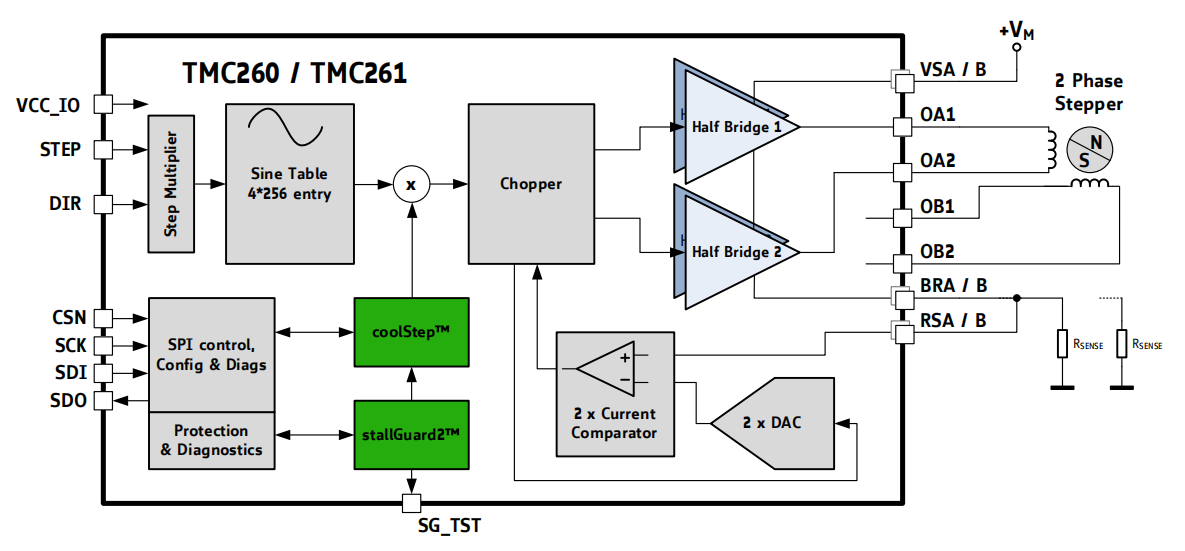
TMC260的架构图
FEATURES AND BENEFITS
- Drive Capability up to 2A motor current
- Highest Voltage up to 60V DC (TMC261) or 40V DC (TMC260)
- Highest Resolution up to 256 microsteps per full step
- Compact Size 10x10mm QFP-44 package
- Low Power Dissipation, low RDSON & synchronous rectification
- EMI-optimized programmable slope
- Protection & Diagnostics overcurrent, short to GND, overtemperature & undervoltage
- stallGuard2™ high precision sensorless motor load detection
- coolStep™ load dependent current control for energy savings up to 75%
- microPlyer™ microstep interpolation for increased smoothness with coarse step inputs
- spreadCycle™ high-precision chopper for best current sine wave form and zero crossing
TMC2660参数
Universal, cost-effective stepper driver for two-phase bipolar motors with state-of-the-art features.
Integrated MOSFETs for up to 4 A motor current per coil. With Step/Dir Interface and SPI.
TMC2660的架构与TMC260的相同。
TMC262参数
Universal, cost-effective stepper driver for two-phase bipolar motors with state-of-the-art features.
External MOSFETs fit different motor sizes. With Step/Dir Interface and SPI.
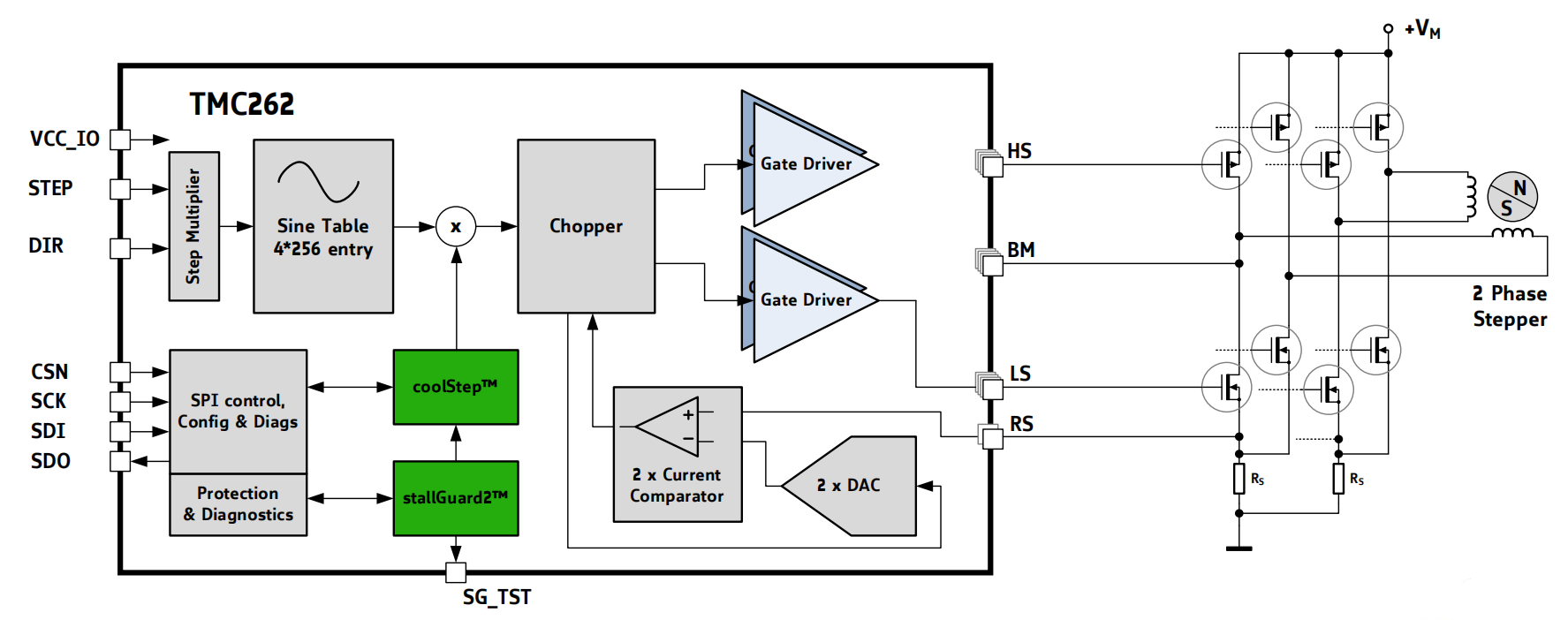
TMC262的架构图
FEATURES AND BENEFITS
- High Motor Current up to 10A using external (N&P) MOSFETs.
- Highest Voltage up to 60V DC operating voltage
- Highest Resolution up to 256 microsteps per full step
- Small Size 5x5mm QFN32 package
- Low Power Dissipation synchronous rectification
- EMI-optimized slope & current controlled gate drivers
- Protection & Diagnostics short to GND, overtemperature & undervoltage; short to VS & overcurrent (TMC262C only)
- StallGuard2™ high precision sensorless motor load detection
- CoolStep™ load dependent current control saves up to 75%
- MicroPlyer™ 256 microstep smoothness with 1/16 step input.
- SpreadCycle™ high-precision chopper for best current sine wave form and zero crossing
- Improved Silent Motor operation (TMC262C only)
- Clock Failsafe option for external clock (TMC262C only)
TMC2160参数
Universal high voltage driver for two-phase bipolar stepper motor. stealthChop™ for quiet movement. External MOSFETs for up to 20A motor current per coil. With Step/Dir Interface and SPI.
TMC2209参数
Step/Dir Drivers for Two-Phase Bipolar Stepper Motors up to 2.8A peak – StealthChop™ for Quiet Movement – UART Interface Option – Sensorless Stall Detection StallGuard4
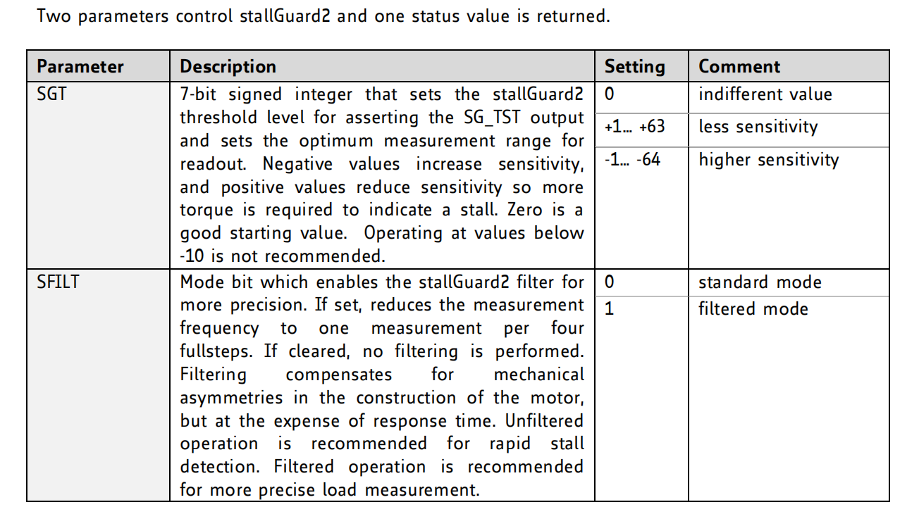
负载测量 - stallGuard2 Load Measurement
stallGuard2 provides an accurate measurement of the load on the motor. It can be used for stall detection as well as other uses at loads below those which stall the motor, such as coolStep load adaptive current reduction. (stallGuard2 is a more precise evolution of the earlier stallGuard technology.)
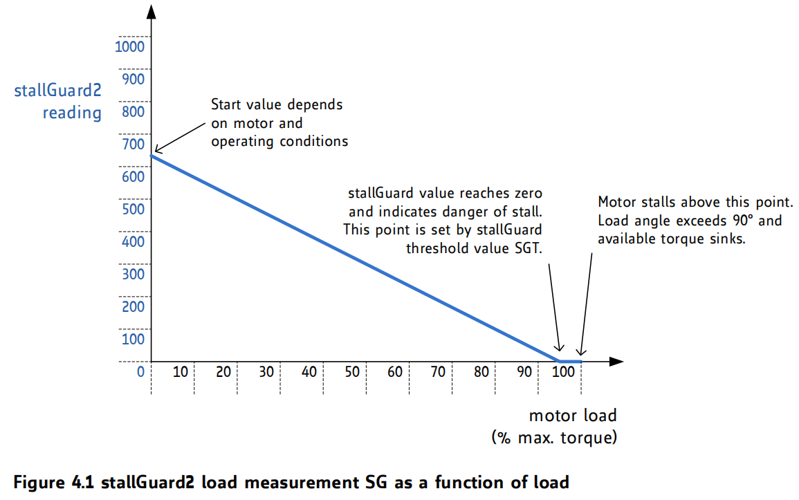
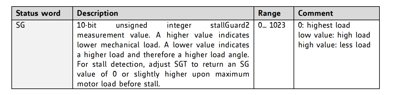
The stallGuard2 measurement value changes linearly over a wide range of load, velocity, and current settings, as shown in Figure 4.1. At maximum motor load, the value goes to zero or near to zero. This corresponds to a load angle of 90° between the magnetic field of the coils and magnets in the rotor. This also is the most energy-efficient point of operation for the motor
coolStep Current Control
coolStep is controlled by several parameters, but two are critical for understanding how it works:
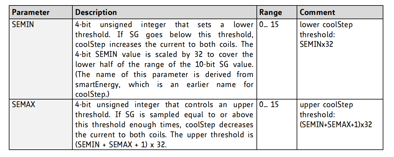
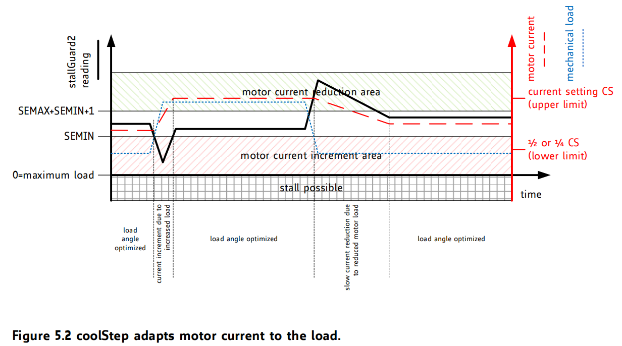
Figure 5.2 shows the operating regions of coolStep. The black line represents the SG measurement value, the blue line represents the mechanical load applied to the motor, and the red line represents the current into the motor coils. When the load increases, SG falls below SEMIN, and coolStep increases the current. When the load decreases and SG rises above (SEMIN + SEMAX + 1) x 32 the current becomes reduced.
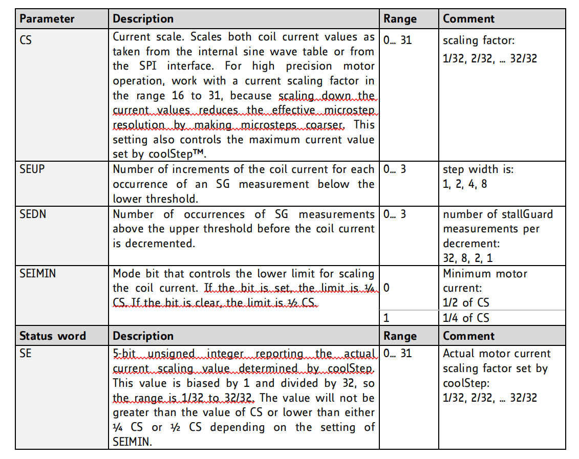
Four more parameters control coolStep and one status value is returned:
SPI Interface
SPI slaves can be chained and used with a single chip select line. If slaves are chained, they behave like a long shift register. For example, a chain of two motor drivers requires 40 bits to be sent. The last bits shifted to each register in the chain are loaded into an internal register on the rising edge of the CSN input. For example, 24 or 32 bits can be sent to a single motor driver, but it latches just the last 20 bits received before CSN goes high.
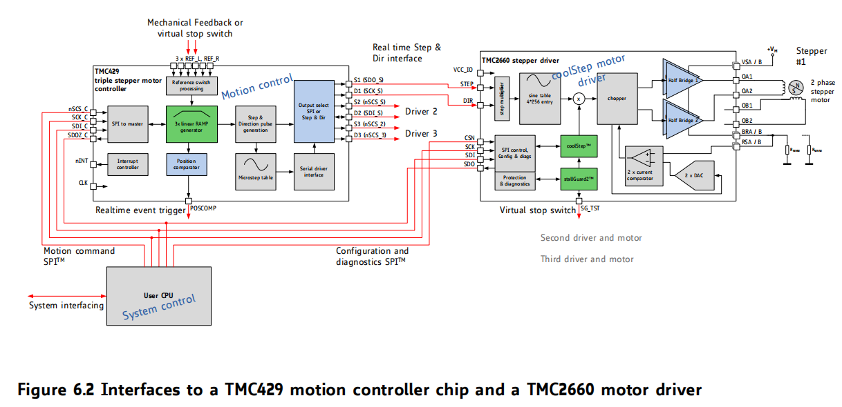
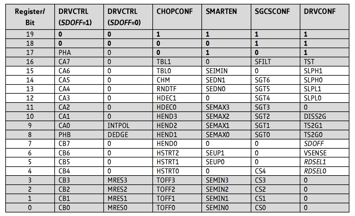
Register Write Commands
An SPI bus transaction to the TMC2660 is a write command to one of the five write-only registers that hold configuration parameters and mode bits:
| Register | Description |
|---|---|
| Driver Control Register (DRVCTRL) | The DRVCTRL register has different formats for controlling the interface to the motion controller depending on whether or not the STEP/DIR interface is enabled. |
| Chopper Configuration Register (CHOPCONF) | The CHOPCONF register holds chopper parameters and mode bits. |
| coolStep Configuration Register (SMARTEN) | The SMARTEN register holds coolStep parameters and a mode bit. (smartEnergy is an earlier name for coolStep.) |
| stallGuard2 Configuration Register (SGCSCONF) | The SGCSCONF register holds stallGuard2 parameters and a mode bit. |
| Driver Configuration Register (DRVCONF) | The DRVCONF register holds parameters and mode bits used to control the power MOSFETs and the protection circuitry. It also holds the SDOFF bit which controls the STEP/DIR interface and the RDSEL parameter which controls the contents of the response returned in an SPI transaction |
Write Command Overview
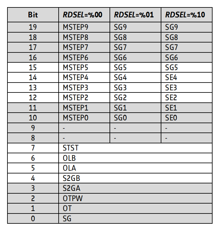
Read Response Overview
- RDSEL: The RDSEL parameter in the DRVCONF register selects the format of the read response.
电流设定与计算
电路设计示例
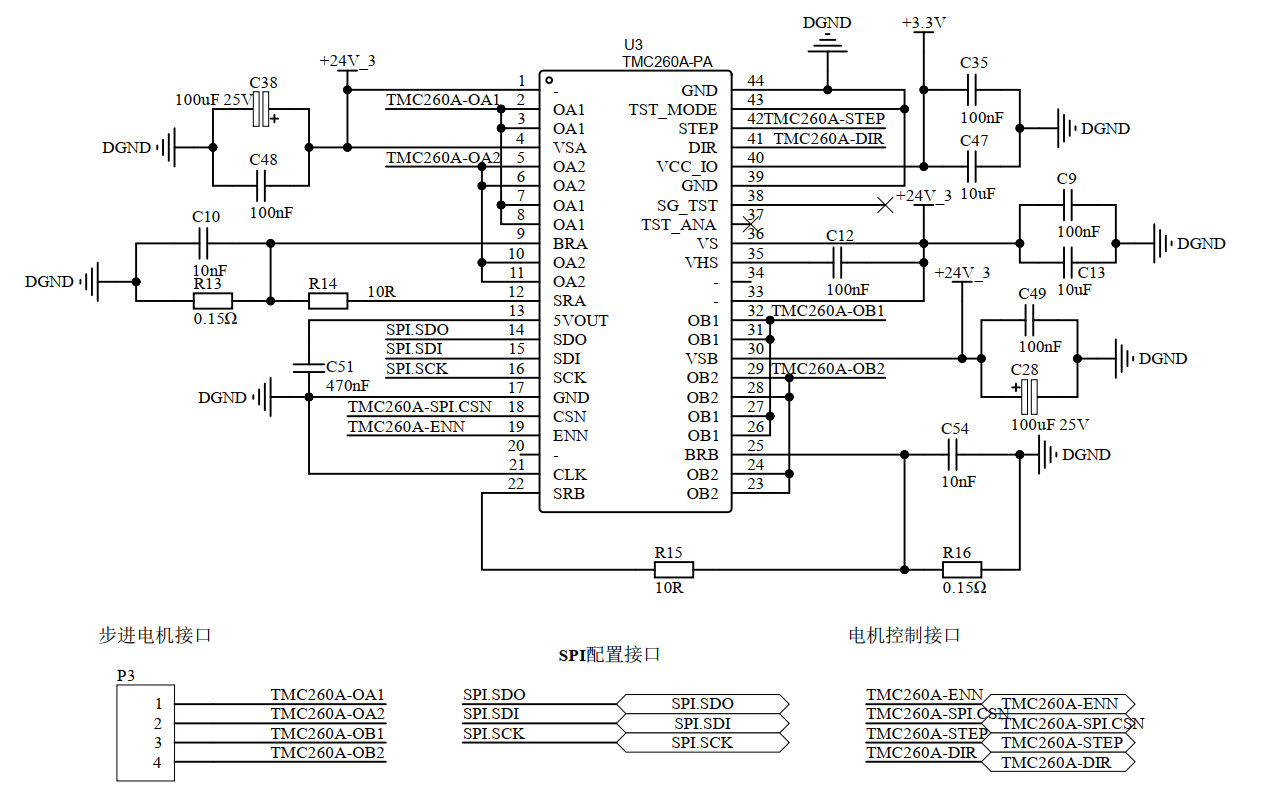
内置MOS管 - TMC260/2660
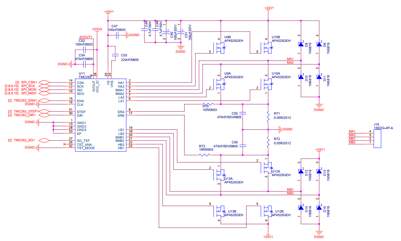
外置MOS管 - TMC262
电流采样电阻设置
根据数据手册,平均电流 I R M S = C S + 1 32 ∗ V F S R s e n s e ∗ 1 2 I_{RMS}=\frac{CS+1}{32}*\frac{V_{FS}}{R_{sense}}*\frac{1}{\sqrt{2}} IRMS=32CS+1∗RsenseVFS∗21,其中 V F S V_{FS} VFS由软件设置,可以选择165mV与310mV。
- 如果 V F S = 310 m V V_{FS}=310mV VFS=310mV 、采样电阻为50mΩ,则 I R M S = C S + 1 32 ∗ 4.384 ( A ) I_{RMS}=\frac{CS+1}{32}*4.384(A) IRMS=32CS+1∗4.384(A)
- 如果 V F S = 310 m V V_{FS}=310mV VFS=310mV 、采样电阻为75mΩ,则 I R M S = C S + 1 32 ∗ 2.923 ( A ) I_{RMS}=\frac{CS+1}{32}*2.923(A) IRMS=32CS+1∗2.923(A)
- 如果 V F S = 310 m V V_{FS}=310mV VFS=310mV 、采样电阻为150mΩ,则 I R M S = C S + 1 32 ∗ 1.461 ( A ) I_{RMS}=\frac{CS+1}{32}*1.461(A) IRMS=32CS+1∗1.461(A)
软件开发示例
驱动程序
头文件tmc260_user.h
/*
 * tmc260.h
 *
 *	本驱动适合TMC260(内置MOS管,2A)/TMC2660(内置MOS管,4A)/TMC262(外置MOS管)系列的步进电机驱动芯片
 *	不同的驱动芯片MOS管位置不一样,且额定电流大小不一样,所配套的电流采样电阻阻值也不同
 *
 *	本驱动主要实现对TMC260等芯片的初始化配置,例如设定细分和电流。对于步进电机的操作控制,请直接使用stepmotor库
 *
 *  Created on: Jun 2, 2020
 *      Author: 81001
 */

#ifndef __TMC260_H__
#define __TMC260_H__

#include "platform.h"

/**
 * Bits 19, 18, and sometimes 17 select the register being written
 * ----------------------------------------------------------------------------------------------------------------------------------
 * Register/Bit		DRVCTRL (SDOFF=1)		DRVCTRL (SDOFF=0)		CHOPCONF				SMARTEN				SGCSCONF		DRVCONF
 * ----------------------------------------------------------------------------------------------------------------------------------
 * 19 						0 						0 					1						1					1				1
 * 18						0						0 					0 						0 					1 				1
 * 17 						PHA 					0 					0 						1 					0 				1
 * 16 						CA7  					0 					TBL1 					0 					SFILT 			TST
 * 15 						CA6  					0 					TBL0 				SEIMIN 					0 				SLPH1
 * 14 						CA5 					0 					CHM 				SEDN1 					SGT6 			SLPH0
 * 13 						CA4  					0 					RNDTF 				SEDN0 					SGT5 			SLPL1
 * 12 						CA3 					0 					HDEC1 				0 						SGT4 			SLPL0
 * 11 						CA2  					0 					HDEC0 				SEMAX3					SGT3 			0
 * 10 						CA1 					0 					HEND3 				SEMAX2 					SGT2 			DISS2G
 * 9 						CA0  					INTPOL				HEND2 				SEMAX1 					SGT1 			TS2G1
 * 8 						PHB  					DEDGE 				HEND1 				SEMAX0 					SGT0 			TS2G0
 * 7 						CB7  					0 					HEND0 				0 						0 				SDOFF
 * 6 						CB6  					0 					HSTRT2 				SEUP1 					0 				VSENSE
 * 5 						CB5  					0 					HSTRT1 				SEUP0 					0 				RDSEL1
 * 4 						CB4  					0 					HSTRT0 				0 						CS4 			RDSEL0
 * 3 						CB3  					MRES3 				TOFF3 				SEMIN3 					CS3 			0
 * 2 						CB2  					MRES2 				TOFF2 				SEMIN2 					CS2 			0
 * 1						CB1  					MRES1 				TOFF 1 				SEMIN1 					CS1 			0
 * 0						CB0  					MRES0 				TOFF0 				SEMIN0					CS0 			0
 * -----------------------------------------------------------------------------------------------------------------------------------
 */

/**
 * ---------------------------------------------REG_DRVCTRL--------------------------------------------------------------------------------------
 * Driver Control Register
 * The DRVCTRL register has different formats for controlling the interface to the motion controller depending on whether or not the STEP/DIR interface is enabled.
 */
#define REG_DRVCTRL			0x00000000			//b0000

/// Enable STEP interpolation (Bit9)
/// 0: Disable STEP pulse interpolation.
/// 1: Enable STEP pulse multiplication by 16.
#define TMC260_REG_DRVCTRL_INTPOL			(0x00000001<<9)

/// Enable double edge STEP pulses (Bit8)
/// 0: Rising STEP pulse edge is active, falling edge is inactive.
/// 1: Both rising and falling STEP pulse edges are active.
#define TMC260_REG_DRVCTRL_DEDGE_PUL			(0x00000000<<8)
#define TMC260_REG_DRVCTRL_DEDGE_REVE			(0x00000001<<8)

/// Microstep resolution (Bit0~3)
/// Microstep resolution for STEP/DIR mode
#define		TMC260_REG_DRVCTRL_MICROSTEP_256			0x00000000
#define		TMC260_REG_DRVCTRL_MICROSTEP_128			0x00000001
#define		TMC260_REG_DRVCTRL_MICROSTEP_64				0x00000002
#define		TMC260_REG_DRVCTRL_MICROSTEP_32				0x00000003
#define		TMC260_REG_DRVCTRL_MICROSTEP_16				0x00000004
#define		TMC260_REG_DRVCTRL_MICROSTEP_8				0x00000005
#define		TMC260_REG_DRVCTRL_MICROSTEP_4				0x00000006
#define		TMC260_REG_DRVCTRL_MICROSTEP_2				0x00000007
#define		TMC260_REG_DRVCTRL_MICROSTEP_1				0x00000008

/**
 * ---------------------------------------------REG_CHOPCONF--------------------------------------------------------------------------------------
 * Chopper Configuration Register
 * The CHOPCONF register holds chopper parameters and mode bits.
 */
#define REG_CHOPCONF		0x00080000			//b1000

/// Blanking time (bit15~16)
/// Blanking time interval, in system clock periods:
/// 00: 16,01: 24,10: 36,11: 54
#define TMC260_REG_CHOPCONF_TBL_16							(0x00000000<<15)
#define TMC260_REG_CHOPCONF_TBL_24							(0x00000001<<15)
#define TMC260_REG_CHOPCONF_TBL_36							(0x00000002<<15)
#define TMC260_REG_CHOPCONF_TBL_54							(0x00000003<<15)

/// Chopper mode (bit14)
/// This mode bit affects the interpretation of the HDEC, HEND, and HSTRT parameters shown below.
/// 0: Standard mode (spreadCycle)
/// 1: Constant tOFF with fast decay time.
/// 		Fast decay time is also terminated when the negative nominal current is reached. Fast decay is after on time.
#define TMC260_REG_CHOPCONF_CHM								(0x00000001<<14)

/// Random TOFF time (bit13)
/// Enable randomizing the slow decay phase duration:
/// 0: Chopper off time is fixed as set by bits tOFF
/// 1: Random mode, tOFF is random modulated by dNCLK= -12 … +3 clocks
#define TMC260_REG_CHOPCONF_RNDTF							(0x00000001<<13)

/// Hysteresis decrement interval or Fast decay mode (bit11~12)
/// CHM=0, Hysteresis decrement period setting, in system clock periods:
/// 00: 16,01: 32,10: 48,11: 64
/// CHM=1, HDEC1=0: current comparator can terminate the fast decay phase before timer expires.
/// 			HDEC1=1: only the timer terminates the fast decay phase.
/// 			HDEC0: MSB of fast decay time setting.
#define TMC260_REG_CHOPCONF_HDEC_00							(0x00000000<<11)
#define TMC260_REG_CHOPCONF_HDEC_01							(0x00000001<<11)
#define TMC260_REG_CHOPCONF_HDEC_10							(0x00000002<<11)
#define TMC260_REG_CHOPCONF_HDEC_11							(0x00000003<<11)

/// Hysteresis end (low) value or Sine wave offset (bit7~10)
/// CHM=0: 0000~1111:  Hysteresis is -3, -2, -1, 0, 1, …, 12
/// (1/512 of this setting adds to current setting)
/// This is the hysteresis value which becomes used for the hysteresis chopper.
#define TMC260_REG_CHOPCONF_HEND_VAL_M3						(0x00000000<<7)
#define TMC260_REG_CHOPCONF_HEND_VAL_0						(0x00000003<<7)

/// Hysteresis start value or Fast decay time setting (bit4~6)
/// CHM=0: Hysteresis start offset from HEND:
/// 		000: 1		100: 5
/// 		001: 2		101: 6
/// 		010: 3		110: 7
///			011: 4		111: 8
/// CHM=1: Three least-significant bits of the duration of the fast decay phase. The MSB is HDEC0.
/// Fast decay time is a multiple of system clock periods: NCLK= 32 x (HDEC0+HSTRT)
#define TMC260_REG_CHOPCONF_HSTRT_000						(0x00000000<<4)
#define TMC260_REG_CHOPCONF_HSTRT_VAL_4					(0x00000003<<4)

/// Off time/MOSFET disable  (bit0~3)
/// Duration of slow decay phase.
/// If TOFF is 0, the MOSFETs are shut off.
/// If TOFF is nonzero, slow decay time is a multiple of system clock periods:
/// NCLK= 12 + (32 x TOFF) (Minimum time is 64clocks.)
/// 0000: Driver disable, all bridges off
/// 0001: 1 (use with TBL of minimum 24 clocks)
/// 0010~1111: 2~15
#define TMC260_REG_CHOPCONF_TOFF_OFF						(0x00000000)
#define TMC260_REG_CHOPCONF_TOFF_B0001						(0x00000001)
#define TMC260_REG_CHOPCONF_TOFF_VAL_8						(0x00000008)

/**
 * ---------------------------------------------REG_SMARTEN--------------------------------------------------------------------------------------
 * coolStep Configuration Register
 * The SMARTEN register holds coolStep parameters and a mode bit. (smartEnergy is an earlier name for coolStep.)
 */
#define REG_SMARTEN			(0x000A0000)			//b1010

/// Minimum coolStep current (bit 15)
/// 0: ½ CS current setting
/// 1: ¼ CS current setting
#define TMC260_REG_SMARTEN_SEIMIN_1_2CS						(0x00000000<<15)
#define TMC260_REG_SMARTEN_SEIMIN_1_4CS						(0x00000001<<15)

/// Current decrement speed (bit 13~14)
/// Number of times that the stallGuard2 value must be sampled equal to or above the upper threshold for each decrement of the coil current:
/// 00: 32, 01: 8, 10: 2, 11: 1
#define TMC260_REG_SMARTEN_SEDN_32							(0x00000000<<13)
#define TMC260_REG_SMARTEN_SEDN_8								(0x00000001<<13)
#define TMC260_REG_SMARTEN_SEDN_2								(0x00000002<<13)
#define TMC260_REG_SMARTEN_SEDN_1								(0x00000003<<13)

/// Upper coolStep threshold as an offset from the lower threshold (bit 8~11)
/// If the stallGuard2 measurement value SG is sampled equal to or above (SEMIN+SEMAX+1) x 32 enough times, then the coil current scaling factor is decremented.
#define TMC260_REG_SMARTEN_SEMAX_B0000						(0x00000000<<8)
#define TMC260_REG_SMARTEN_SEMAX_B0010						(0x00000002<<8)

/// Current increment size (bit 5~6)
/// Number of current increment steps for each time that the stallGuard2 value SG is sampled below the lower threshold:
#define TMC260_REG_SMARTEN_SEUP_1							(0x00000000<<5)
#define TMC260_REG_SMARTEN_SEUP_2							(0x00000001<<5)
#define TMC260_REG_SMARTEN_SEUP_4							(0x00000002<<5)
#define TMC260_REG_SMARTEN_SEUP_8							(0x00000003<<5)

/// Lower coolStep threshold / coolStep disable (bit 0~3)
/// If SEMIN is 0, coolStep is disabled. If SEMIN is nonzero and the stallGuard2 value SG falls below SEMIN x 32, the coolStep current scaling factor is increased.
#define TMC260_REG_SMARTEN_SEMIN_COOL_DISABLE				(0x00000000)
#define TMC260_REG_SMARTEN_SEMIN_B0010						(0x00000002)

/**
 * -----------------------------------------------------------------------------------------------------------------------------------
 * stallGuard2 Configuration Register
 * The SGCSCONF register holds stallGuard2 parameters and a mode bit.
 */
#define REG_SGCSCONF		0x000C0000			//b1100

/// stallGuard2 filter enable (bit 16)
/// 0: Standard mode, fastest response time.
/// 1: Filtered mode, updated once for each four fullsteps to compensate for variation in motor construction, highest accuracy.
#define 		TMC260_REG_SGCSCONF_SFILT_STD							(0x00000000<<16)
#define 		TMC260_REG_SGCSCONF_SFILT_FILT							(0x00000001<<16)

/// stallGuard2 threshold value (bit 8~14)
/// The stallGuard2 threshold value controls the optimum measurement range for readout.
/// A lower value results in a higher sensitivity and requires less torque to indicate a stall.
/// The value is a two’s complement signed integer. Values below -10 are not recommended.
/// Range: -64 to +63
#define 		TMC260_REG_SGCSCONF_SGT_B0000000						(0x00000000<<8)

/// Current scale (scales digital currents A and B) (bit 0~4)
/// 00000~11111: 1/32, 2/32, 3/32, … 32/32
/// This value is biased by 1 and divided by 32, so the range is 1/32 to 32/32. Example: CS=0 is 1/32 current.
#define 		TMC260_REG_SGCSCONF_CS_B00000							(0x00000000)
#define 		TMC260_REG_SGCSCONF_CS_VAL_20_32						(0x00000013)
#define 		TMC260_REG_SGCSCONF_CS_VAL_16_32						(0x0000000F)
#define 		TMC260_REG_SGCSCONF_CS_VAL_32_32						(0x0000001F)

/**
 * -----------------------------------------------------------------------------------------------------------------------------------
 * Driver Configuration Register
 * The DRVCONF register holds parameters and mode bits used to control the power MOSFETs and the protection circuitry.
 * It also holds the SDOFF bit which controls the STEP/DIR interface and the RDSEL parameter which controls the contents of the response returned in an SPI transaction.
 */
#define REG_DRVCONF			0X000E0000			//b1110

/// Reserved TEST mode (bit 16)
/// Must be cleared for normal operation.
/// When set, the SG_TST output exposes digital test values, and the TEST_ANA output exposes analog test values.
/// Test value selection is controlled by SGT1 and SGT0:
/// TEST_ANA: 00: anatest_2vth, 01: anatest_dac_out, 10: anatest_vdd_half.
/// SG_TST: 00: comp_A, 01: comp_B, 10: CLK, 11: on_state_xy
#define TMC260_REG_DRVCONF_TST												(0x00000000<<16)

/// Slope control, high side (bit 14~15)
/// 00: Minimum
/// 01: Minimum temperature compensation mode.
/// 10: Medium temperature compensation mode.
/// 11: Maximum
/// In temperature compensated mode (tc), the MOSFET gate driver strength is increased if the overtemperature warning temperature is reached.
/// This compensates for temperature dependency of high-side slope control.
#define TMC260_REG_DRVCONF_SLPH_MIN										(0x00000000<<14)
#define TMC260_REG_DRVCONF_SLPH_MIN_TC									(0x00000001<<14)
#define TMC260_REG_DRVCONF_SLPH_MED_TC									(0x00000002<<14)
#define TMC260_REG_DRVCONF_SLPH_MAX										(0x00000003<<14)

/// Slope control, low side (bit 12~13)
/// 00: Minimum
/// 01: Minimum temperature compensation mode.
/// 10: Medium temperature compensation mode.
/// 11: Maximum
#define TMC260_REG_DRVCONF_SLPL_MIN                                  		(0x00000000<<12)
#define TMC260_REG_DRVCONF_SLPL_MIN_TC                               	(0x00000001<<12)
#define TMC260_REG_DRVCONF_SLPL_MED_TC                               	(0x00000002<<12)
#define TMC260_REG_DRVCONF_SLPL_MAX                                  	(0x00000003<<12)

/// Short to GND protection disable (bit 10)
#define TMC260_REG_DRVCONF_DISS2G_ENABLE								(0x00000000<<10)
#define TMC260_REG_DRVCONF_DISS2G_DISABLE							(0x00000001<<10)

/// Short to GND detection timer (bit 8~9)
#define TMC260_REG_DRVCONF_TS2G_3_2US									(0x00000000<<8)
#define TMC260_REG_DRVCONF_TS2G_1_6US									(0x00000001<<8)
#define TMC260_REG_DRVCONF_TS2G_1_2US									(0x00000002<<8)
#define TMC260_REG_DRVCONF_TS2G_0_8US									(0x00000003<<8)

/// STEP/DIR interface disable (bit7)
/// 0: Enable STEP and DIR interface.
/// 1: Disable STEP and DIR interface. SPI interface is used to move motor.
#define TMC260_REG_DRVCONF_SDOF_EN_STEP								(0x00000000<<7)
#define TMC260_REG_DRVCONF_SDOF_DISEN_STEP							(0x00000001<<7)

/// Sense resistor voltage-based current scaling (bit 6)
/// 0: Full-scale sense resistor voltage is 305mV.
/// 1: Full-scale sense resistor voltage is 165mV.
/// (Full-scale refers to a current setting of 31 and a DAC value of 255.)
#define TMC260_REG_DRVCONF_VSENSE_305MV								(0x00000000<<6)
#define TMC260_REG_DRVCONF_VSENSE_165MV								(0x00000001<<6)

/// Select value for read out (RD bits) (bit: 4~5)
/// 00: Microstep position read back
/// 01: stallGuard2 level read back
/// 10: stallGuard2 and coolStep current level read back
/// 11: Reserved, do not use
#define TMC260_REG_DRVCONF_RDSEL_B00										(0x00000000<<4)
#define TMC260_REG_DRVCONF_RDSEL_B01										(0x00000001<<4)
#define TMC260_REG_DRVCONF_RDSEL_B10										(0x00000002<<4)
#define TMC260_REG_DRVCONF_RDSEL_B11										(0x00000003<<4)

typedef struct
{
	SPI_TypeDef *SPIx;
	uint32_t *Pin_CS;
}TMC260_TypeDef;

/**
 * @brief 电机驱动器初始化
 * @param tmc260 电机驱动器结构体
 */
void TMC260_Init(TMC260_TypeDef *tmc260);

/**
 * @brief 设置电机的工作电流(1/32~32/32)
 * @param curr 1~32 (I = curr/32 * 310mv/R)
 */
void TMC260_SetCurrent(TMC260_TypeDef *tmc260, uint8_t curr);

/**
 * @brief 设置电机驱动器的细分
 * @param subdivi 电机的细分,可以取值的选项有1, 2, 4, 8, 16, 32, 64, 128, 256
 */
void TMC260_SetSubdivision(TMC260_TypeDef *tmc260, uint16_t subdivi);

/**
 * @brief 获取电机驱动器的状态信息
 * @param tmc260 电机驱动器结构体
 * @return uint32_t 堵转数值(Stall Value)
 */
uint32_t TMC260_ReadState(TMC260_TypeDef *tmc260);

/**
 * @brief 向电机驱动器传输数据
 * @param tmc260 电机驱动器结构体
 * @param write_data 写入的数据
 * @return uint32_t 读出的数据
 */
uint32_t TMC260_SPI_TransData(TMC260_TypeDef *tmc260, uint32_t write_data);

#endif /* _TMC260_H_ */
源文件tmc260_user.c
/*
 * tmc260.c
 *
 *  Created on: Jun 2, 2020
 *      Author: 81001
 */

#include "tmc260.h"
#include "spi_ext.h"

/**
 * @brief 电机驱动器初始化
 * @param tmc260 电机驱动器结构体
 */
void TMC260_Init(TMC260_TypeDef *tmc260)
{
	//Configure of REG_DRVCONF (2A * 150 mohm = 300 mV)
	TMC260_SPI_TransData(tmc260, REG_DRVCONF | TMC260_REG_DRVCONF_RDSEL_B01 | TMC260_REG_DRVCONF_VSENSE_305MV);

	//Configure of REG_DRVCONF
	TMC260_SPI_TransData(tmc260, REG_DRVCTRL | TMC260_REG_DRVCTRL_DEDGE_PUL | TMC260_REG_DRVCTRL_MICROSTEP_8);

	//Configure of CHOPCONF
	TMC260_SPI_TransData(tmc260, REG_CHOPCONF | TMC260_REG_CHOPCONF_TBL_36 | TMC260_REG_CHOPCONF_HEND_VAL_0 | TMC260_REG_CHOPCONF_HSTRT_VAL_4 | TMC260_REG_CHOPCONF_TOFF_VAL_8);

	//Configure of REG_SGCSCONF
	TMC260_SPI_TransData(tmc260, REG_SGCSCONF | TMC260_REG_SGCSCONF_CS_VAL_16_32);

	//coolStep Configuration Register
	TMC260_SPI_TransData(tmc260, REG_SMARTEN | TMC260_REG_SMARTEN_SEIMIN_1_2CS | TMC260_REG_SMARTEN_SEDN_32 | TMC260_REG_SMARTEN_SEMAX_B0010 | TMC260_REG_SMARTEN_SEMIN_B0010);
}

/**
 * @brief 设置电机驱动器的最大电流
 * @param curr 1~32 (I = curr/32 * 310mv/R, 1/32~32/32)
 */
void TMC260_SetCurrent(TMC260_TypeDef *tmc260, uint8_t curr)
{
	if(curr > 32)
	{
		curr = 32;
	}
	else if (curr < 1)
	{
		curr = 1;
	}
	else
	{

	}

	TMC260_SPI_TransData(tmc260, REG_SGCSCONF | TMC260_REG_SGCSCONF_SFILT_FILT | (curr-1) );
}

/**
 * @brief 设置电机驱动器的细分
 * @param subdivi 电机的细分,可以取值的选项有1, 2, 4, 8, 16, 32, 64, 128, 256
 */
void TMC260_SetSubdivision(TMC260_TypeDef *tmc260, uint16_t subdivi)
{
	uint32_t cmd = 0;
	switch(subdivi)
	{
	case 1:
		cmd = 8;
		break;
	case 2:
		cmd = 7;
		break;
	case 4:
		cmd = 6;
		break;
	case 8:
		cmd = 5;
		break;
	case 16:
		cmd = 4;
		break;
	case 32:
		cmd = 3;
		break;
	case 64:
		cmd = 2;
		break;
	case 128:
		cmd = 1;
		break;
	case 256:
		cmd = 0;
		break;
	default:
		return;
	}

	TMC260_SPI_TransData(tmc260, REG_DRVCTRL | TMC260_REG_DRVCTRL_DEDGE_PUL | cmd);
}

/**
 * @brief 获取电机驱动器的状态信息
 * @param tmc260 电机驱动器结构体
 * @return uint32_t 堵转数值(Stall Value)
 */
uint32_t TMC260_ReadState(TMC260_TypeDef *tmc260)
{
	uint32_t Sta_Val = 0;
	Sta_Val = TMC260_SPI_TransData(tmc260, REG_SMARTEN | TMC260_REG_SMARTEN_SEIMIN_1_2CS | TMC260_REG_SMARTEN_SEDN_32 | TMC260_REG_SMARTEN_SEMAX_B0010 | TMC260_REG_SMARTEN_SEMIN_B0010);

	return Sta_Val >> 10;
}

/**
 * @brief 向电机驱动器传输数据
 * @param tmc260 电机驱动器结构体
 * @param write_data 写入的数据
 * @return uint32_t 读出的数据
 */
uint32_t TMC260_SPI_TransData(TMC260_TypeDef *tmc260, uint32_t write_data)
{
	uint8_t send_buff[3], recv_buff[3];
	uint32_t recv_data = 0;

	*tmc260->Pin_CS = 0;

	send_buff[0] = (write_data >> 16) & 0xff;
	send_buff[1] = (write_data >> 8) & 0xff;
	send_buff[2] = (write_data & 0xff);

	SPI_TransData(tmc260->SPIx, send_buff, recv_buff, 3);

	recv_data = recv_buff[0] << 16 | recv_buff[1] << 8 | recv_buff[2];

	*tmc260->Pin_CS = 1;

	return (recv_data & 0x0fffff);
}
配置程序
头文件tmc260_user.h
/*
 * tmc260_user.h
 *
 *  Created on: Jun 2, 2020
 *      Author: 81001
 */

#ifndef _TMC260_USER_H_
#define _TMC260_USER_H_

#include "tmc260.h"
#include "gpio_ext.h"

#define TMC2660_1_CS_ADDR					GPIOE_OUT_ADDR(1)
#define TMC2660_2_CS_ADDR					GPIOE_OUT_ADDR(6)
#define TMC2660_3_CS_ADDR					GPIOE_OUT_ADDR(11)
#define TMC2660_4_CS_ADDR					GPIOD_OUT_ADDR(8)

#define TMC2660_1_GET_SUBDIV                HoldingReg_GetData_Float(0)
#define TMC2660_1_GET_MAXCURR               HoldingReg_GetData_Float(1)

#define TMC2660_2_GET_SUBDIV                HoldingReg_GetData_Float(2)
#define TMC2660_2_GET_MAXCURR               HoldingReg_GetData_Float(3)

#define TMC2660_3_GET_SUBDIV                HoldingReg_GetData_Float(4)
#define TMC2660_3_GET_MAXCURR               HoldingReg_GetData_Float(5)

#define TMC2660_4_GET_SUBDIV                HoldingReg_GetData_Float(6)
#define TMC2660_4_GET_MAXCURR               HoldingReg_GetData_Float(7)

// #define TMC2660_1_SG_ADDR					GPIOB_IN_ADDR(12)

extern TMC260_TypeDef Tmc260Array[4];

void TMC260_UserInit();

#endif /* _INC_TMC260_H_ */
用户源文件tmc260_user.c
/*
 * tmc260_user.c
 *
 *  Created on: Jun 2, 2020
 *      Author: 81001
 */

#include "tmc260_user.h"
#include "mb_user.h"

TMC260_TypeDef Tmc260Array[4] = {
	{.Pin_CS = TMC2660_1_CS_ADDR, .SPIx = SPI1, },
	{.Pin_CS = TMC2660_2_CS_ADDR, .SPIx = SPI1, },
	{.Pin_CS = TMC2660_3_CS_ADDR, .SPIx = SPI1, },
	{.Pin_CS = TMC2660_4_CS_ADDR, .SPIx = SPI1, },
};

void TMC260_UserInit()
{
	TMC260_Init(&Tmc260Array[0]);
	TMC260_SetSubdivision(&Tmc260Array[0], TMC2660_1_GET_SUBDIV);
	TMC260_SetCurrent(&Tmc260Array[0], TMC2660_1_GET_MAXCURR);

	TMC260_Init(&Tmc260Array[1]);
	TMC260_SetSubdivision(&Tmc260Array[1], TMC2660_2_GET_SUBDIV);
	TMC260_SetCurrent(&Tmc260Array[1], TMC2660_2_GET_MAXCURR);

	TMC260_Init(&Tmc260Array[2]);
	TMC260_SetSubdivision(&Tmc260Array[2], TMC2660_3_GET_SUBDIV);
	TMC260_SetCurrent(&Tmc260Array[2], TMC2660_3_GET_MAXCURR);

	TMC260_Init(&Tmc260Array[3]);
	TMC260_SetSubdivision(&Tmc260Array[3], TMC2660_4_GET_SUBDIV);
	TMC260_SetCurrent(&Tmc260Array[3], TMC2660_4_GET_MAXCURR);
}
用户程序
TMC系列芯片完成配置后,用户程序主要是通过标准的Dir、Pul、En接口实现对步进电机的控制。对步进电机的控制请参考“步进电机驱动库”。
- 在用户业务初始化函数中实现对TMC系列芯片的初始化
void User_Init()
{
	Filter_MovingAverage_Init();

	// Set the slave address
	MB_CommParam.MB_SlaveAddr = Debug_GetDipSwitchValue(DIPSW_GpioArray, DIPSW_GPIOARRAY_LEN, 0);

	// 将 限位开关触发处理 注册为 外部中断回调函数
	EXTI_0_Triggered = User_Limit_1_SwitchHandler;
	EXTI_1_Triggered = User_Limit_1_SwitchHandler;
	EXTI_2_Triggered = User_Limit_1_SwitchHandler;
	EXTI_3_Triggered = User_Limit_1_SwitchHandler;

	EXTI_4_Triggered = User_Limit_2_SwitchHandler;
	EXTI_5_Triggered = User_Limit_2_SwitchHandler;
	EXTI_6_Triggered = User_Limit_2_SwitchHandler;
	EXTI_7_Triggered = User_Limit_2_SwitchHandler;

	EXTI_8_Triggered = User_Limit_3_SwitchHandler;
	EXTI_9_Triggered = User_Limit_3_SwitchHandler;
	EXTI_10_Triggered = User_Limit_3_SwitchHandler;
	EXTI_11_Triggered = User_Limit_3_SwitchHandler;

	EXTI_12_Triggered = User_Limit_4_SwitchHandler;
	EXTI_13_Triggered = User_Limit_4_SwitchHandler;
	EXTI_14_Triggered = User_Limit_4_SwitchHandler;
	EXTI_15_Triggered = User_Limit_4_SwitchHandler;

	// 初始化Modbus的寄存器
	User_MB_InitRegs();

	// 初始化TMC系列芯片
	TMC260_UserInit();

	// 初始化步进电机
	StepMotor_InitAll();
- 在任务轮询中实时修改、读取TMC系列芯片的参数(电机电流、细分、负载值等)
/**
 * @brief 刷新输入寄存器,将传感器数据赋值到输入寄存器
 * @param none
 * @retval none
 */
void User_MB_RefreshInputRegister()
{
	uint32_t stall1 = TMC260_ReadState(&Tmc260Array[0]);
	uint32_t stall2 = TMC260_ReadState(&Tmc260Array[1]);
	uint32_t stall3 = TMC260_ReadState(&Tmc260Array[2]);
	uint32_t stall4 = TMC260_ReadState(&Tmc260Array[3]);

	InputReg_SetData_Float(5, stall1);
	InputReg_SetData_Float(6, stall2);
	InputReg_SetData_Float(7, stall3);
	InputReg_SetData_Float(8, stall4);
}

/**
 * @brief Refresh holding registers
 */
void User_MB_RefreshHoldingRegister()
{
	static float holdingRegBuff_SMConf[8] = {-1, -1, -1, -1, -1, -1, -1, -1};

	// TMC262的参数设定发生变化,立即更新生效
	for (uint8_t i = 0; i < 4; i++)
	{
		// 电机细分参数发生改变
		if(holdingRegBuff_SMConf[2*i] != HoldingReg_GetData_Float(2*i))
		{
			holdingRegBuff_SMConf[2*i] = HoldingReg_GetData_Float(2*i);
			TMC260_SetSubdivision(&Tmc260Array[i], holdingRegBuff_SMConf[2*i]);
		}

		// 电机电流参数发生改变
		if(holdingRegBuff_SMConf[2*i+1] != HoldingReg_GetData_Float(2*i+1))
		{
			holdingRegBuff_SMConf[2*i+1] = HoldingReg_GetData_Float(2*i+1);
			TMC260_SetCurrent(&Tmc260Array[i], holdingRegBuff_SMConf[2*i+1]);
		}
	}
}


 9437
9437


 被折叠的 条评论
为什么被折叠?
被折叠的 条评论
为什么被折叠?
 到【灌水乐园】发言


