


根据前两节课,我们明白不同内存类设备与2440的连接
2440与NOR flash的连接图


 由上图NOR flash 读的时序图可知,Taa即当输出地址的70ns之后数据有效;Tce即当CE处于低电平大于70ns之后数据有效;Toe即当OE处于低电平大于30ns之后数据有效;Trc即为读周期的时间为70ns;Tdf即为OE和CE处于高电平大于30ns之后,数据输出稳定;综上,我们要让2440同时发出CE,OE,addr信号。

寄存器的配置:
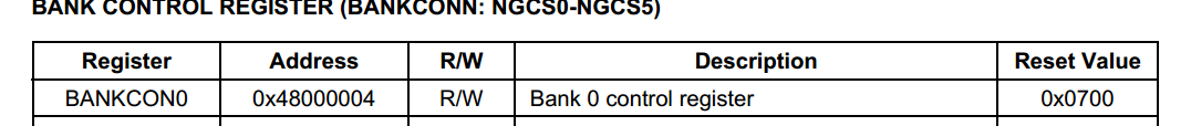

综上,通过配置寄存器BANKCON0使其发出可以满足控制NOR flash读的时序
代码
init.c

#include "s3c2440_soc.h"

void bank0_tacc_set(int val)
{
	BANKCON0 = val << 8;
}

init.h

#ifndef _INIT_H
#define _INIT_H

void bank0_tacc_set(int val);

#endif

main.c

#include "s3c2440_soc.h"
#include "uart.h"
#include "init.h"

int main(void)
{
	unsigned char c;

	uart0_init();
	puts("Enter the Tacc val: \n\r");

	while(1)
	{
		c = getchar();
		putchar(c);
		if (c >= '0' && c <= '7')
		{
			bank0_tacc_set(c - '0');
			led_test();
		}
		else
		{
			puts("Error, val should between 0~7\n\r");
			puts("Enter the Tacc val: \n\r");
		}
	}
	return 0;
}


 2万+
2万+


 被折叠的 条评论
为什么被折叠?
被折叠的 条评论
为什么被折叠?
 到【灌水乐园】发言


