


Title: A Novel Segmented Modeling Method of Via including the Effect of Power/Ground Plane Pair
Author: ZhaowenYan,ZhicaiMa,GuochangShi,and MingmingChe
purpose: The main purpose of the passage is to present and validate a novel segmented modeling method for vias in printed circuit boards (PCBs) that includes the effects of power and ground plane pairs. This method aims to enhance the accuracy and efficiency of modeling high-frequency interconnect structures, which is crucial for maintaining signal integrity, power integrity, and electromagnetic compatibility in modern high-speed electronic systems. The passage describes the methodology, highlights the advantages over existing methods, and demonstrates the effectiveness of the proposed approach through comparison with full-wave simulation results.
Generally Summarize the paper
Abstract
- The paper focuses on a novel modeling method for common interconnects in PCBs, emphasizing fast modeling and parameter extraction using the cavity resonance method.本文重点介绍一种用于 PCB 中常见互连的新型建模方法,重点介绍使用腔体谐振法进行快速建模和参数提取。
- The segmented via modeling method includes the effect of power/ground plane pairs.分段通孔建模方法包括电源/接地平面对的影响。
- The method decomposes the via structure into three parts, modeling each part separately.该方法将通孔结构分解为三个部分,对每个部分分别进行建模。
- High accuracy is achieved using a second-order circuit model for capacitance and inductance, validated by simulation results within 9GHz.使用二阶电路模型对电容和电感实现了高精度计算,并通过 9GHz 内的仿真结果进行了验证。
- An equivalent circuit model of a signal network is established and co-simulated, showing consistent results with HFSS simulations.建立了信号网络的等效电路模型并进行了联合仿真,结果与 HFSS 仿真结果一致。
Introduction
- Discusses the importance of accurate interconnect modeling in GHz and UHF frequency ranges due to the increasing density and speed of modern circuits.讨论了由于现代电路密度和速度的不断增加,在 GHz 和 UHF 频率范围内进行精确互连建模的重要性。
- Highlights the significance of power distribution networks (PDNs) in PCB layouts and their impact on signal transmission quality.强调了电源分配网络 (PDN) 在 PCB 布局中的重要性及其对信号传输质量的影响。
- Points out the necessity of accurate via modeling to mitigate signal integrity issues in high-frequency circuits.指出了精确的通孔建模对于缓解高频电路中的信号完整性问题的必要性。
More specifically
- Importance of Interconnect Modeling: As electronic circuits operate at higher frequencies, accurate modeling of interconnects like vias becomes critical to ensure signal integrity, power integrity, and electromagnetic compatibility.由于电子电路在更高频率下工作,对通孔等互连进行准确建模对于确保信号完整性、电源完整性和电磁兼容性至关重要。
- Power Distribution Networks (PDNs): The paper emphasizes that the power distribution network (PDN) in a PCB significantly affects signal transmission quality. Understanding and modeling the impedance and resonance characteristics of PDNs are essential for high-fidelity circuit design.PCB 中的电源分配网络 (PDN) 会显著影响信号传输质量。理解和建模 PDN 的阻抗和谐振特性对于高保真电路设计至关重要。
- Existing Modeling Methods: The introduction reviews existing via modeling approaches, highlighting their limitations:
- Quasistatic methods are accurate at low frequencies but not suitable for high-frequency applications.准静态方法在低频下准确,但不适用于高频应用。
- Full-wave simulations, while highly accurate, are computationally intensive and time-consuming.全波模拟虽然高度准确,但计算量大且耗时。
- Some fast modeling techniques compromise on accuracy.一些快速建模技术会牺牲准确性。
- Need for a Novel Method: The introduction argues for the need for a method that balances accuracy and computational efficiency, leading to the proposed segmented modeling method.需要一种平衡准确性和计算效率的方法,从而提出了分段建模方法。
Additional Details
- Challenges in Modeling: The introduction discusses the complexities involved in modeling the electromagnetic behavior of vias and the surrounding PDN in high-frequency circuits. It underscores the need for methods that can accurately predict these behaviors to prevent signal integrity problems like reflection, crosstalk, and noise.引言讨论了在高频电路中对通孔和周围 PDN 的电磁行为进行建模所涉及的复杂性。它强调需要能够准确预测这些行为的方法,以防止反射、串扰和噪声等信号完整性问题。
- Segmentation Approach: The novel approach proposed involves segmenting the via structure into distinct parts, each modeled separately to improve overall accuracy. This method leverages the cavity resonance technique to account for the power/ground plane effects, which are crucial at high frequencies.提出的新方法涉及将通孔结构分割成不同的部分,每个部分单独建模以提高整体准确性。该方法利用腔体共振技术来解释电源/接地平面效应,这在高频下至关重要。
Modeling of Power/Ground Plane Pair
-
Resonance Characteristics of Plane Pair:
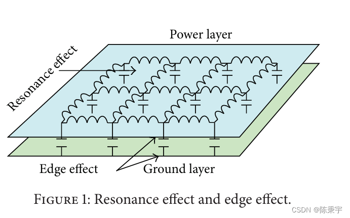
- Power and ground plane pairs in a PCB can behave like resonant cavities.PCB 中的电源和接地平面对可以表现得像谐振腔。
- The resonant frequencies and the impedance characteristics of these planes can significantly affect signal integrity.这些平面的谐振频率和阻抗特性会显著影响信号完整性。
-
Cavity Resonance Method:
- The paper uses the cavity resonance method to model the impedance of the power/ground plane pair.本文使用腔体谐振方法来建模电源/接地平面对的阻抗。
- This method considers the planes as a cavity with specific boundary conditions, such as Perfect Electric Conductor (PEC), Perfect Magnetic Conductor (PMC), and Perfectly Matched Layer (PML).该方法将平面视为具有特定边界条件的腔体,例如完美电导体边界 (PEC)、完美磁导体边界 (PMC) 和完美匹配层边界(PML)。
- PEC(完美磁导体边界),可以用于建模一个有限的电开路平行板。PMC(完美电导体边界),可以用于建模一个有限的电短路平行板。PML(完美匹配层边界),可以用于建模一个无限板或者平行板,可以视为无限。
- 下图为一对矩形电源/接地平面,为方便描述各种物理参数,将其置于三维笛卡尔坐标系中,以板底顶点为坐标原点,平行板的长度为a,宽度为b,介质厚度为h,两者的位置坐标为
,
。
- 对于 PEC 和 PMC 边界,平行板的阻抗:
-
Impedance Calculation:
- This involves determining the resonant frequencies and corresponding impedance characteristics.这涉及确定谐振频率和相应的阻抗特性。
- The results from this calculation are incorporated into the segmented via model to enhance its accuracy.此计算的结果被纳入分段通孔模型以提高其准确性。
-
Modeling Techniques:
- Rectangular Plane Pair: The study focuses on modeling a rectangular power/ground plane pair.矩形平面对:本研究重点是建模矩形电源/接地平面对。
- Boundary Conditions: Different boundary conditions are applied to accurately capture the resonance behavior.边界条件:应用不同的边界条件来准确捕捉谐振行为。
- Analytical Formulas: The paper uses analytical formulas to calculate the input impedance at various frequencies.解析公式:本文使用解析公式来计算不同频率下的输入阻抗。
Segmented Modeling Method of Via
-
Overview of Segmented Modeling:
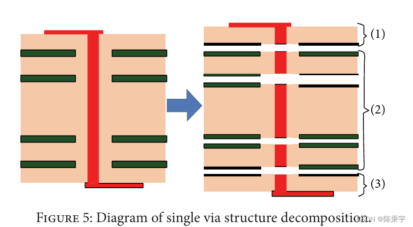
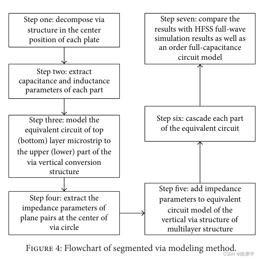
- The via structure is divided into three distinct segments to simplify the modeling process and improve accuracy.通孔结构被分为三个不同的部分,以简化建模过程并提高准确性。
- Each segment is analyzed separately, and their combined effects are integrated into a comprehensive via model.每个部分都单独进行分析,并将它们的组合效果集成到一个综合通孔模型中。
-
Segmentation of the Via Structure:
- Top-Level Transmission Line to Via: This segment includes the transition from the transmission line on the top layer of the PCB to the via.顶层传输线到通孔:此段包括从 PCB 顶层的传输线到通孔的过渡。
- Middle Multilayer Via Structure: This segment covers the via itself as it passes through the various layers of the PCB.中间多层通孔结构:此段覆盖通孔本身,因为它穿过 PCB 的各个层。
- Bottom-Level Via to Transmission Line: This segment includes the transition from the via to the transmission line on the bottom layer of the PCB.底层通孔到传输线:此段包括从通孔到 PCB 底层的传输线的过渡。
-
Modeling Each Segment:
- Each segment is modeled using an LC second-order circuit to capture the inductance (L) and capacitance (C) effects accurately.每个段都使用 LC 二阶电路进行建模,以准确捕捉电感 (L) 和电容 (C) 效应。
- The segmented approach allows for detailed modeling of each part, considering its specific electrical characteristics.分段方法允许对每个部分进行详细建模,同时考虑其特定的电气特性。
-
Incorporation of Impedance Effects:
- The impedance of the power/ground plane pairs, calculated using the cavity resonance method, is integrated into the segmented via model. 使用腔体谐振方法计算的电源/接地平面对的阻抗被集成到分段通孔模型中。
- This integration ensures that the resonance effects of the PDN are accurately reflected in the via model.这种集成确保 PDN 的谐振效应准确反映在通孔模型中。
-
LC Second-Order Circuit Model:
- Each segment is represented by an LC circuit model, which includes inductance and capacitance elements to simulate the high-frequency behavior of the via.每个段都由一个 LC 电路模型表示,其中包括电感和电容元件,以模拟通孔的高频行为。
- The second-order model provides higher accuracy than first-order models, especially in capturing resonant effects.二阶模型比一阶模型提供更高的精度,尤其是在捕捉谐振效应方面。
Examples of Segmented Modeling of Via
-
Overview of Examples:
- The section presents specific examples of via structures and applies the segmented modeling method to them.本节介绍通孔结构的具体示例,并将分段建模方法应用于这些示例。
- The purpose is to illustrate the practical application of the method and to validate its accuracy through comparison with full-wave simulation results.目的是说明该方法的实际应用,并通过与全波仿真结果进行比较来验证其准确性。
-
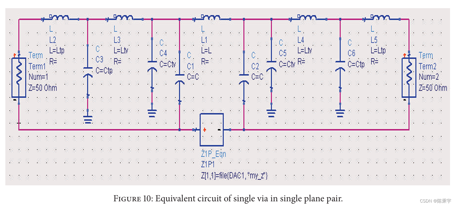
Example 1: Single Via in a Simple PCB Structure:
- Description: The first example might involve a single via in a basic PCB layout with power and ground planes.说明:第一个示例可能涉及具有电源和接地平面的基本 PCB 布局中的单个通孔。
- Segmentation: The via is segmented into the top-level transmission line to via, the middle multilayer via structure, and the bottom-level via to transmission line.分段:通孔被分段为顶层传输线到通孔、中间多层通孔结构和底层通孔到传输线。
- Modeling: Each segment is modeled using the LC second-order circuit model.建模:每个段都使用 LC 二阶电路模型进行建模。
- Results: The impedance and resonance characteristics are calculated and compared with full-wave simulation results from HFSS.结果:计算阻抗和谐振特性,并与 HFSS 的全波仿真结果进行比较。
-
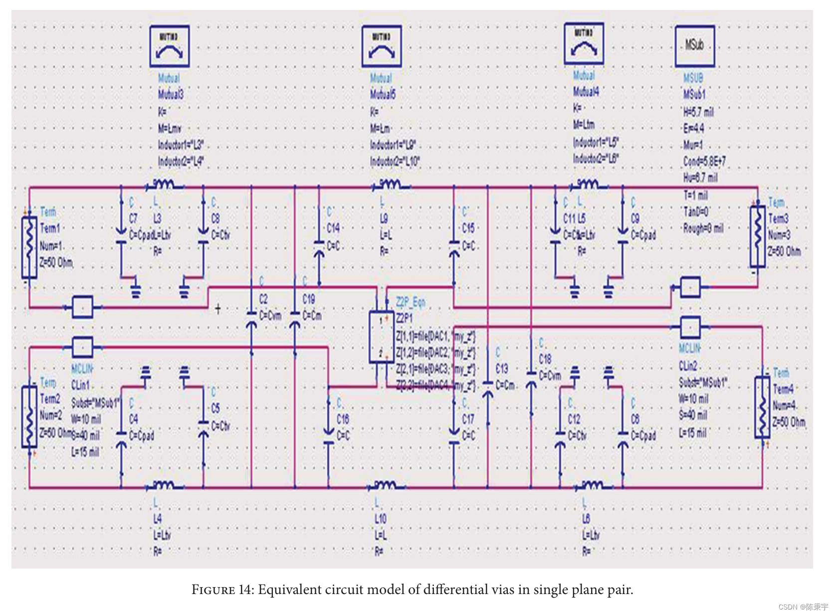
Example 2: Differential Vias in a Complex PCB Structure:
- Description: The second example might involve differential vias in a more complex multilayer PCB with multiple power and ground planes.说明:第二个示例可能涉及具有多个电源和接地平面的更复杂的多层 PCB 中的差分通孔。
- Segmentation: The differential vias are segmented similarly to the single via example, with additional considerations for the differential signal paths.分段:差分通孔的分段类似于单通孔示例,但还考虑了差分信号路径。
- Modeling: Each segment for the differential vias is modeled, incorporating the effects of the power/ground plane pairs.建模:对差分过孔的每个部分进行建模,并结合电源/接地平面对的影响。
- Results: The results are compared with full-wave simulations to validate the accuracy of the segmented modeling method.结果:将结果与全波仿真进行比较,以验证分段建模方法的准确性。
-
Comparison with Full-Wave Simulations:
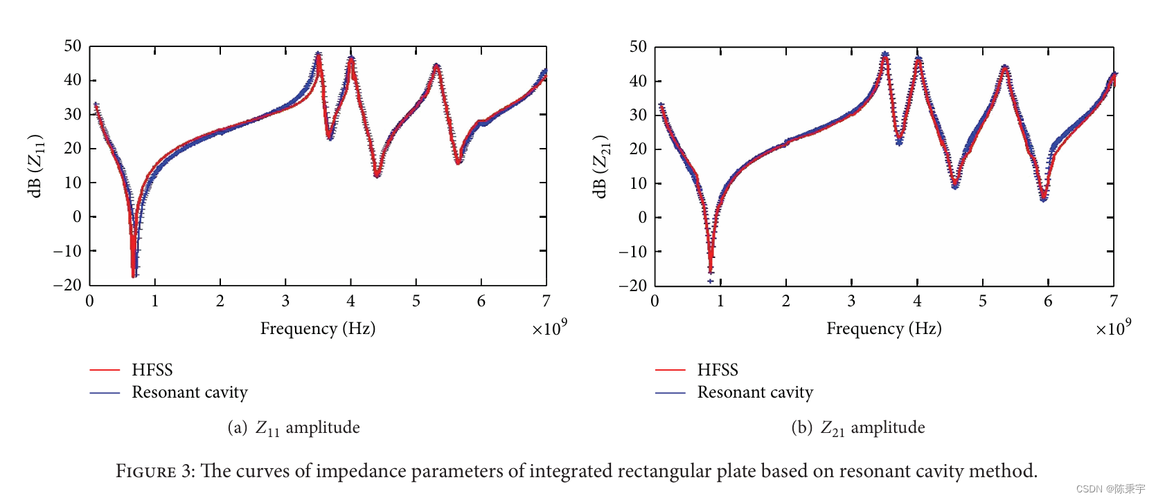
- The results from the segmented modeling method are compared with full-wave simulation results from HFSS to validate the accuracy.将分段建模方法的结果与 HFSS 的全波仿真结果进行比较,以验证准确性。
- The comparisons show good agreement, demonstrating the reliability and effectiveness of the proposed method.比较结果显示出良好的一致性,证明了所提方法的可靠性和有效性。
- This validation step is crucial to confirm that the segmented modeling method can accurately predict the impedance and resonance characteristics of vias in high-frequency PCB designs.此验证步骤对于确认分段建模方法可以准确预测高频 PCB 设计中过孔的阻抗和谐振特性至关重要。
Comprehensive Modeling Method of Coupled Channels
-
Importance of Modeling Coupled Channels:
- In high-density PCBs, signal traces and vias are often placed close to each other, leading to electromagnetic coupling.在高密度 PCB 中,信号走线和过孔通常彼此靠近,从而导致电磁耦合。
- Accurate modeling of these coupled channels is essential to predict and mitigate crosstalk and other signal integrity issues.准确建模这些耦合通道对于预测和缓解串扰和其他信号完整性问题至关重要。
-
Segmentation Approach for Coupled Channels:
- Similar to single vias, coupled channels are segmented into manageable parts for detailed modeling.与单个过孔类似,耦合通道被分段为可管理的部分以进行详细建模。
- Each segment is modeled to capture the individual and mutual impedance characteristics accurately.每个段都经过建模,以准确捕获单个和相互的阻抗特性。
-
LC Circuit Model for Coupled Segments:
- Each segment of the coupled channels is represented by an LC circuit model.耦合通道的每个段都由 LC 电路模型表示。
- Mutual inductance and capacitance are included to account for the coupling effects between channels.包括互感和电容以考虑通道之间的耦合效应。
-
Integration of Power/Ground Plane Effects:
- The impedance effects of the power/ground plane pairs are integrated into the model.电源/接地平面对的阻抗效应被集成到模型中。
- This ensures that the resonance characteristics of the PDN are accurately reflected in the coupled channel model.这确保 PDN 的谐振特性准确反映在耦合通道模型中。
Conclusion
-
Summary of the Research:
- The paper reiterates the challenges of modeling vias accurately in high-frequency PCB designs, emphasizing the limitations of existing methods.本文重申了在高频 PCB 设计中准确建模通孔的挑战,强调了现有方法的局限性。
- It recaps the main goals of the research, which were to develop a method that balances accuracy and computational efficiency.它重述了研究的主要目标,即开发一种平衡准确性和计算效率的方法。
-
Proposed Segmented Modeling Method:
- The conclusion highlights the proposed segmented modeling method, which decomposes the via structure into manageable segments.结论强调了提出的分段建模方法,该方法将通孔结构分解为可管理的段。
- Each segment is modeled using an LC second-order circuit, and the impedance effects of the power/ground plane pairs are incorporated using the cavity resonance method.每个段都使用 LC 二阶电路建模,并使用腔体谐振方法整合电源/接地平面对的阻抗效应。
-
Validation and Results:
- The conclusion summarizes the validation process, noting that the results of the segmented modeling method were compared with full-wave simulation results (e.g., from HFSS).结论总结了验证过程,并指出将分段建模方法的结果与全波仿真结果(例如来自 HFSS)进行了比较。
- It emphasizes the good agreement between the segmented modeling results and the full-wave simulation results, demonstrating the accuracy and reliability of the proposed method.它强调了分段建模结果与全波仿真结果之间的良好一致性,证明了所提方法的准确性和可靠性。
-
Advantages of the Segmented Modeling Method:
- The method offers a significant improvement in computational efficiency while maintaining high accuracy.该方法在保持高精度的同时显著提高了计算效率。
- By segmenting the via structure and accurately modeling each part, the method reduces complexity without sacrificing precision.通过分割通孔结构并精确建模每个部分,该方法降低了复杂性,同时又不牺牲精度。
-
Applications and Implications:
- The conclusion discusses the practical applications of the method in high-frequency and high-speed PCB designs.结论部分讨论了该方法在高频和高速 PCB 设计中的实际应用。
- It highlights the method's potential to improve signal integrity, reduce crosstalk, and optimize power distribution networks.它强调了该方法在改善信号完整性、减少串扰和优化配电网络方面的潜力。
-
Future Work:
- The paper may suggest areas for future research, such as extending the method to more complex via structures or different types of PCBs.本文可能会提出未来研究的领域,例如将该方法扩展到更复杂的通孔结构或不同类型的 PCB。
- It might also propose further validation through experimental measurements or additional simulations.它还可能提出通过实验测量或额外模拟进行进一步验证。
(先写这么多,有些东西自己也还不是特别理解,后面会再优化和补充)


 568
568


 被折叠的 条评论
为什么被折叠?
被折叠的 条评论
为什么被折叠?
 到【灌水乐园】发言


