


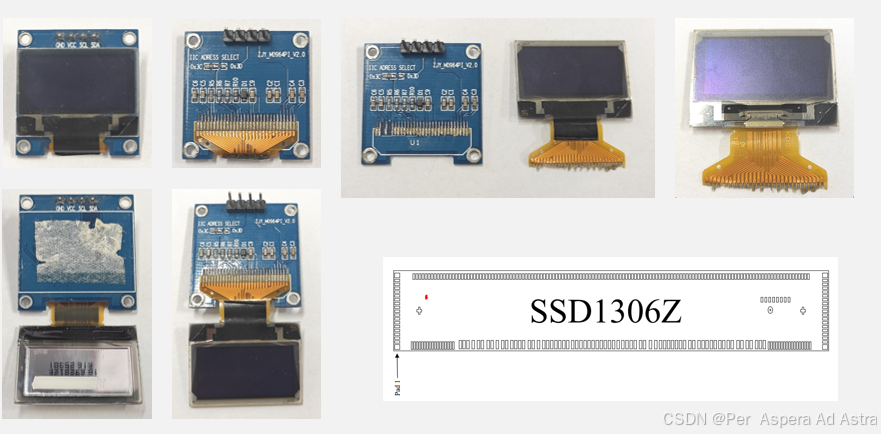
一 、OLED屏幕介绍
OLED,即有机发光二极管( Organic Light Emitting Diode)。 OLED 由于同时具备自发光,不需背光源、对比度高、厚度薄、视角广、反应速度快、可用于挠曲性面板、使用温度范围广、构造及 制程较简单等优异之特性,被认为是下一代的平面显示器新兴应用技术。
LCD 都需要背光,而 OLED 不需要,因为它是自发光的。这样同样的显示 OLED 效果要来得好一 些。以目前的技术,OLED 的尺寸还难以大型化,但是分辨率确可以做到很高。
1.1 特点
- 0.96 寸 OLED 有黄蓝,白,蓝三种颜色可选;其中黄蓝是屏上 1/4 部分为黄光,下 3/4 为蓝; 而且是固定区域显示固定颜色,颜色和显示区域均不能修改;白光则为纯白,也就是黑底白字; 蓝色则为纯蓝,也就是黑底蓝字。
- 分辨率为 128*64
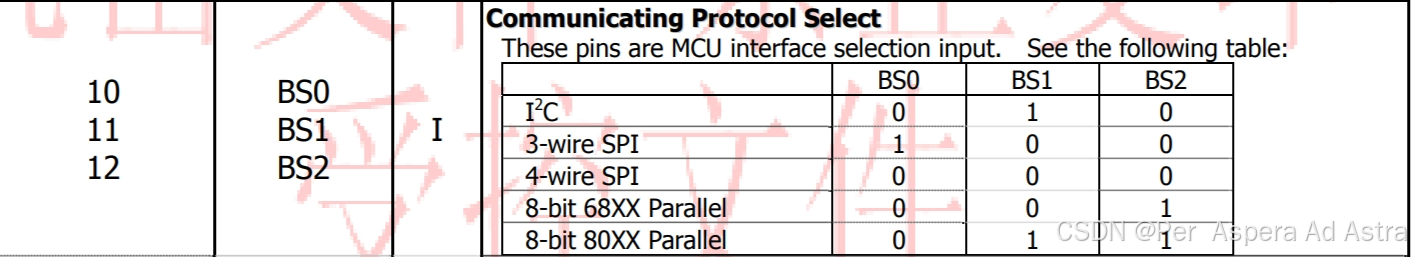
- 多种接口方式;OLED 裸屏总共种接口包括:6800、8080 两种并行接口方式、3 线或 4 线的 串行 SPI 接口方式、 IIC 接口方式(只需要 2 根线就可以控制 OLED 了!),这五种接口是通过 屏上的 BS0~BS2 来配置的。
- 驱动 IC 为 SSD1306,其具有内部升压功能
二、OLED屏幕接口
2.1 SPI接口
模块接口定义:
- 1. GND 电源地
- 2. VCC 电源正(3~5.5V)
- 3. D0 OLED 的 D0 脚,在 SPI 和 IIC 通信中为时钟管脚
- 4. D1 OLED 的 D1 脚,在 SPI 和 IIC 通信中为数据管脚
- 5. RES OLED 的 RES#脚,用来复位(低电平复位)
- 6. DC OLED 的 D/C#E 脚,数据和命令控制管脚
- 7. CS OLED 的 CS#脚,也就是片选管脚
2.2 IIC接口
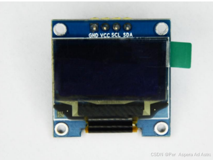
- 1. GND 电源地
- 2. VCC 电源正(3~5.5V)
- 3. SCL OLED 的 D0 脚,在 IIC 通信中为时钟管脚
- 4. SDA OLED 的 D1 脚,在 IIC 通信中为数据管脚
三、OLED驱动 IC --SSD1306简介
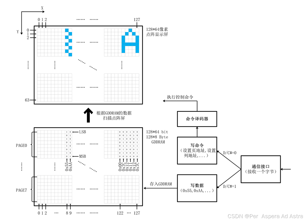
- SSD1306是一款OLED/PLED点阵显示屏的控制器,可以嵌入在屏幕中,用于执行接收数据、显示存储、扫描刷新等任务
- 驱动接口:128个SEG段引脚和64个COM公引脚,对应128*64像素点阵显示屏
- 内置显示存储器(GDDRAM):128*64 bit (128*8 Byte)SRAM
- 供电:VDD=1.65~3.3V(IC 逻辑),VCC=7~15V(面板驱动)
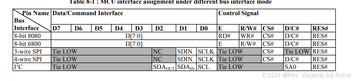
- 通信接口:8位6800/8080并行接口,3/4线SPI接口,I2C接口
- 在串行模式操作中不提供数据读取。
3.1引脚定义
| 引脚 | 功能 |
| VDD、VCC、 VSS、VLSS | 供电 VDD=1.65~3.3V,VCC=7~15V |
| D0~D7 | 6800/8080:8位双向数据总线 3/4线SPI:D0为SCLK,D1为SDIN I2C:D0为SCL,D1为SDAin,D2为SDAout |
| BS0~BS2 | 选择通信接口 |
| R/W#(WR#) | 6800:R/W#,指定读/写操作 8080:WR#,写使能 |
| E(RD#) | 6800:E,读/写使能 8080:RD#,读使能 |
| D/C# | 6800/8080/4线SPI:指定传输数据/指令 I2C:SA0,指定I2C从机地址最低位 |
| CS# | 片选 |
| RES# | 复位 |
3.1.1选择通讯接口
3.1.2不同总线接口模式下的单片机接口分配
SSD1306单片机接口由8个数据引脚和5个控制引脚组成。不同接口模式下的引脚分配情况如下表所示。通过BS[2:0]引脚上的硬件选择可以设置不同的MCU模式
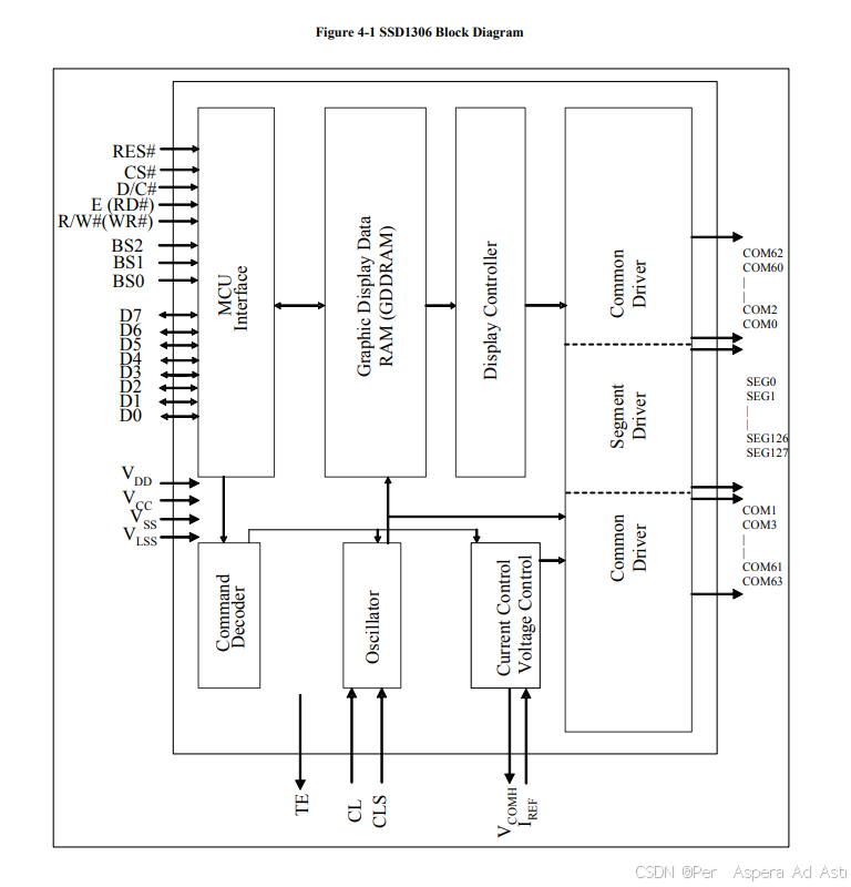
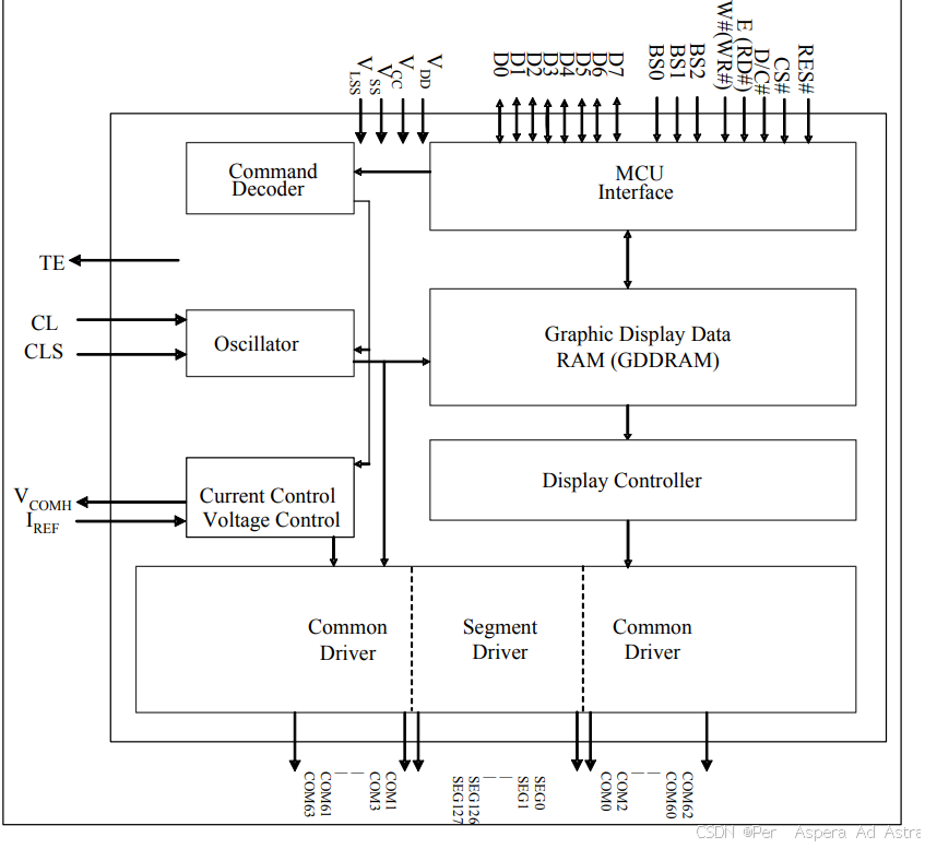
3.2 SSD1306框图
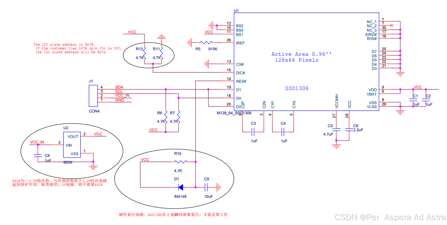
3.3 IIC通讯
4针脚I2C接口模块原理图
3.3.1 从机地址
设备将以以下字节格式响应从地址后面的从地址位(“SA0”位)和读/写选择位(“R/ w#”位):
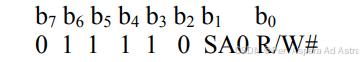
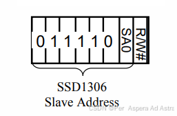
SA0位为从地址提供扩展位,SSD1306的从地址可以选择“0111 100X ”或“0111 101X ”
SA0位为上文3.1.2中的D/C#位
R/W#位决定IIC是读还是写,当为高电平时为读模式,当为低电平时为写模式
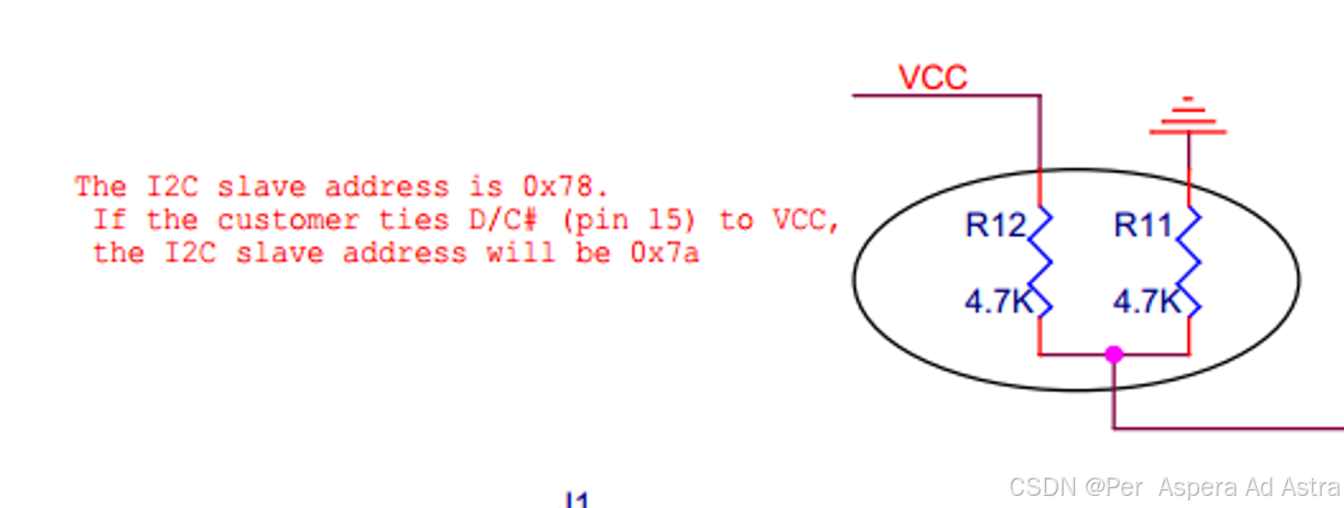
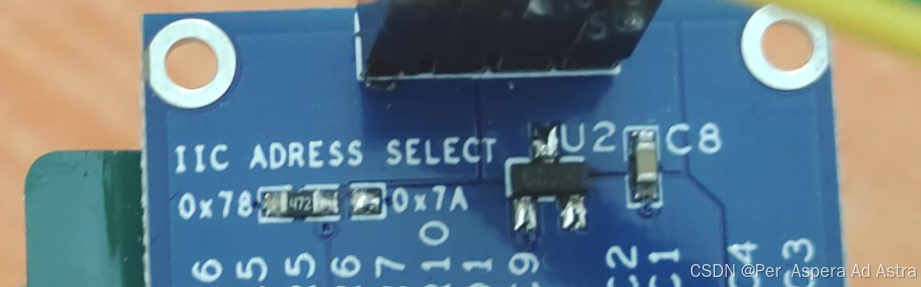
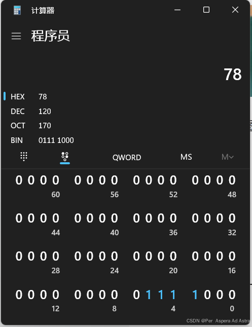
由以上俩张图片可知,OLED默认地址为0X78,当SA0为高电平时地址为0X7A
在串行模式操作中不提供数据读取,因此R/W#为低电平。
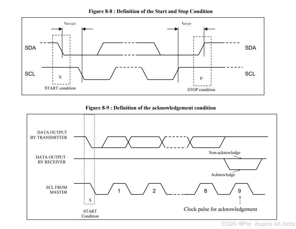
3.3.2 时序
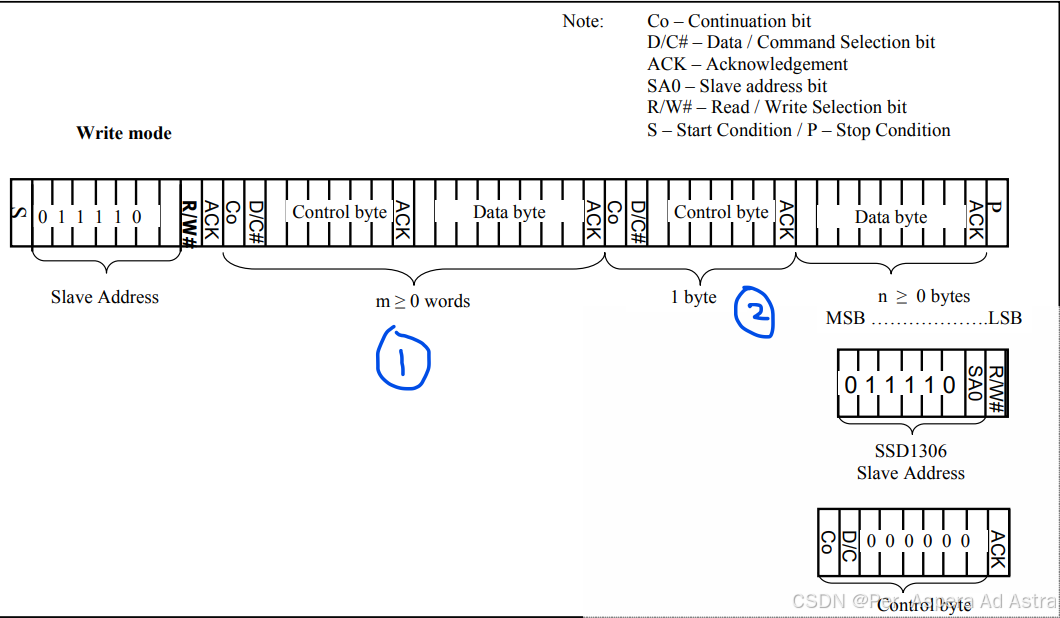
在从地址传输之后,控制字节或数据字节可以通过SDA发送。控制字节主要由Co和D/ c#位组成,后面跟着六个“0”。
C0:连续位-------0 与 1 决定着发送的格式
- 如果将Co位设置为逻辑“0”,则以下信息的传输将只包含数据字节。 控制字节 -- 数据字节 -- 数据字节 -- 数据字节 -- 数据字节 --------
- 如果将Co位设置为逻辑“1”,则以下信息的传输包含控制字节与数据字节。 控制字节 -- 数据字节 -- 控制字节-- 数据字节 -- 控制字节-- 数据字节 -------
D/ c#位决定下一个数据字节作为命令或数据。
- 如果D/ c#位设置为逻辑“0”,则将以下数据字节定义为命令。
- 如果D/ c#位设置为逻辑“1”,则将以下数据字节定义为将存储在GDDRAM中的数据。GDDRAM的列地址指针在每次写数据后自动加1。
3.4 SPI通讯
暂时没用到,以后填坑
3.5 图形显示数据RAM (GDDRAM)
GDDRAM是位映射静态RAM,保存要显示的位模式。RAM的大小为
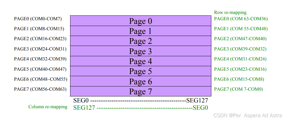
128 × 64位,RAM分为8个页面,从PAGE0到PAGE7,用于单色128x64点阵显示
128*64 bit (128*8 Byte)SRAM
总共64列,使用串行通讯的话一个字节对应于8位,高位先行,所以分为8页
当一个数据字节写入GDDRAM时,将当前列同一页的所有行图像数据全部填充(即填充列地址指针所指向的整列(8位))。如下图所示,D0位写在最上面一行,D7位写在最下面一行。
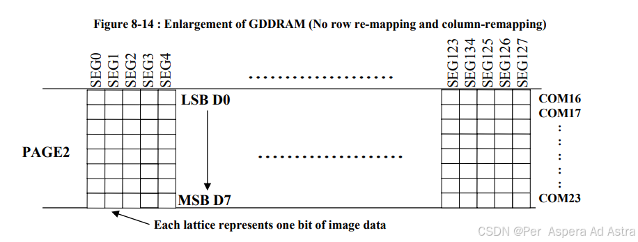
每个格表示一位图像数据
3.6 命令表
- 通过写命令时序传输的字节,作为发送给SSD1306的一个命令
- SSD1306查询命令表的定义,执行相应的操作
- 命令可以由一个字节或者连续的多个字节组成
- 命令可分为基础命令、滚屏命令、寻址命令、硬件配置命令、时间及驱动命令5大类
OLED屏幕常用指令
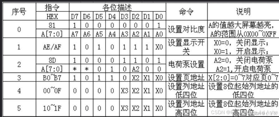
- 命令0X81: 设置对比度。包含两个字节,第一个0X81为命令,随后方法是的一个字节要设置这个对比度,值越大屏幕越亮。
- 命令0XAE/0XAF: 0XAE为关闭显示命令,0XAF为开启显示命令
- 命令0X8D: 包含两个字节,第一个为命令字,第二个为设置值,第二个字节的BIT2表示电荷泵的开关状态,该位为1开启电荷泵,为0则关闭。模块初始化的时候,这个必须要开启,否则看不到屏幕显示。
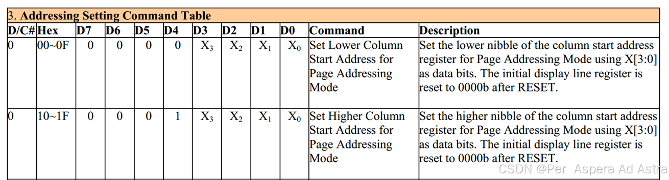
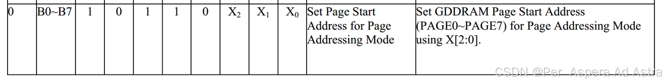
- 命令0XB0~B7:用于设置页地址,其低三位的值对应GRAM页地址。
- 命令0X00~0X0F:用于设置显示时的起始列地址低四位。
- 命令0X10~0X1F: 用于设置显示时的起始列地址高四位。
3.6.1寻址模式(20h)
在SSD1306中有3种不同的内存寻址模式:页寻址模式、水平寻址模式和垂直寻址模式。该命令将内存寻址方式设置为上述三种模式之一。其中,“COL”表示图形显示数据RAM列。
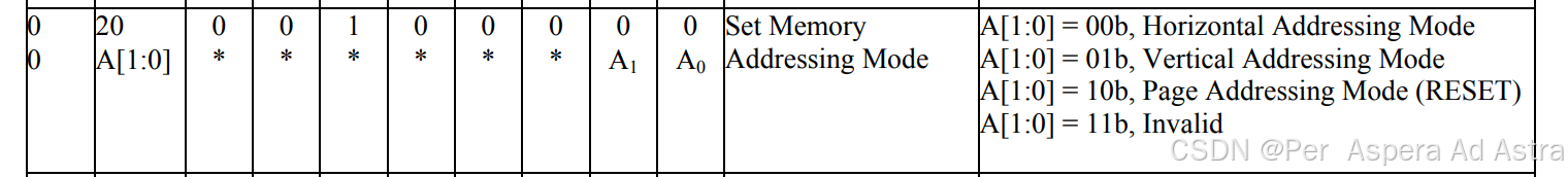
A[1:0] = 00b,水平寻址模式
A[1:0] = 01b,垂直寻址模式
A[1:0] = 10b,页面寻址模式(RESET)
A[1:0] = 11b,无效
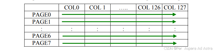
3.6.1.1 页面寻址模式(A[1:0]=10b)
在页寻址模式下,读/写显示RAM后,列地址指针自动增加1。如果列地址指针到达列结束地址,则将列地址指针重置为列开始地址,不修改页面地址指针。用户必须设置新的页和列地址,以便访问下一页RAM内容。页寻址模式下的页和列地址点的移动顺序如图10-1所示。
在正常的显示数据RAM读写和页面寻址模式下,需要通过以下步骤来定义RAM的起始访问指针位置:
- 通过命令B0h到B7h设置目标显示位置的页面起始地址。
- 通过命令00h~0Fh设置指针的下起始列地址。
- 通过命令10h~1Fh设置指针上起始列地址。
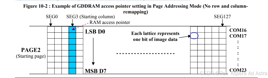
例如,页面地址设置为B2h,下列地址为03h,上列地址为00h,则表示起始列为PAGE2的SEG3。RAM访问指针的位置如图
图10 - 2。输入数据字节将写入第3列的RAM位置。
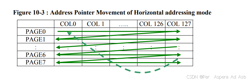
3.6.1.2 水平寻址模式(A[1:0]=00b)
在水平寻址模式下,读/写显示RAM后,列地址指针自动增加1。当列地址指针到达列结束地址时,列地址指针重置为列开始地址,页面地址指针加1。水平寻址方式的页地址点和列地址点的移动顺序如图10-3所示。当列地址指针和页地址指针都到达结束地址时,指针被重置为列起始地址和页起始地址(图10-3虚线)。
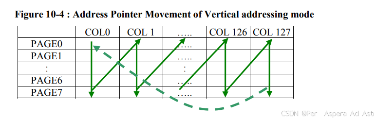
3.6.1.3 垂直寻址模式:(A[1:0]=01b)
在垂直寻址模式下,读/写显示RAM后,页地址指针自动增加1。当页地址指针到达页结束地址时,将页地址指针重置为页起始地址,列地址指针加1。垂直寻址方式的页和列地址点的移动顺序如图10-4所示。当列和页地址指针都到达结束地址时,指针被重置为列起始地址和页起始地址
(如图10-4虚线所示)
四、OLED驱动
4.1 内部DC/DC电路产生的VCC
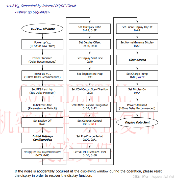
中景园电子提供的OLED配置流程


 2981
2981

 被折叠的 条评论
为什么被折叠?
被折叠的 条评论
为什么被折叠?
 到【灌水乐园】发言


