


 本文详细解析了STM32定时器的输出比较功能,包括如何配置捕获/比较寄存器来实现输出波形控制,设定中断使能,选择输出模式,以及通过更新TIMx_CCRx寄存器控制输出波形。并通过实例说明了如何通过修改CCR值定制方波信号。
1 简介:
This function is used to control an output waveform or indicating when a period of time has elapsed. When a match is found between the capture/compare register TIMx_CCRx and the counter TIMx_ARR,
the output compare function:
• Assigns the corresponding output pin to a programmable value defined by the output compare mode (OCxM bits in the TIMx_CCMRx register) and the output polarity (CCxP bit in the TIMx_CCER register). The output pin can keep its level (OCXM=000), be set active (OCxM=001), be set inactive (OCxM=010) or can toggle (OCxM=011) on match.
TIMx capture/compare mode register 1 (TIMx_CCMR1)
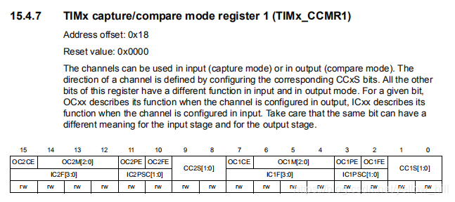
OC1M: Output compare 1 mode
• Sets a flag in the interrupt status register (CCxIF bit in the TIMx_SR register).
• Generates an interrupt if the corresponding interrupt mask is set (CCXIE bit in the TIMx_DIER register).
Bit 1 CC1IE: Capture/Compare 1 interrupt enable
0: CC1 interrupt disabled
1: CC1 interrupt enabled
• Sends a DMA request if the corresponding enable bit is set (CCxDE bit in the TIMx_DIER register, CCDS bit in the TIMx_CR2 register for the DMA request selection).
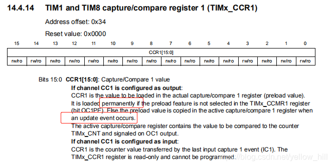
The TIMx_CCRx registers can be programmed with or without preload registers using the OCxPE bit in the TIMx_CCMRx register. In output compare mode, the update event UEV has no effect on OCxREF and OCx output.
The timing resolution is one count of the counter. Output compare mode can also be used to output a single pulse (in One Pulse mode).
2 举例:
Procedure:
1. Select the counter clock (internal, external, prescaler). 选择输入源
2. Write the desired data in the TIMx_ARR and TIMx_CCRx registers. 设定比较的源值到定时器和输入输出比较器
3. Set the CCxIE bit if an interrupt request is to be generated. 中断使能
4. Select the output mode. For example: 设定输出模式
– Write OCxM = 011 to toggle OCx output pin when CNT matches CCRx 设定输出模式,并讲输出匹配到OCx output pin
011: Toggle - OC1REF toggles (接入)when TIMx_CNT=TIMx_CCR1.
– Write OCxPE = 0 to disable preload register
– Write CCxP = 0 to select active high polarity
– Write CCxE = 1 to enable the output 输出使能
5. Enable the counter by setting the CEN bit in the TIMx_CR1 register. 开始计数
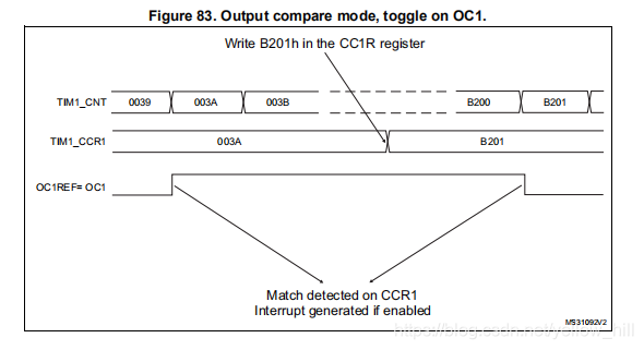
The TIMx_CCRx register can be updated at any time by software to control the output waveform, provided that the preload register is not enabled (OCxPE=’0’, else TIMx_CCRx shadow register is updated only at the next update event UEV). An example is given in
上例小结:
首先,ARR其实为0和CCR的值3A都设定好了,然后,通道设定好,将OC1RE的波形Toggle到OC1,然后,设置CEN开始计数,计数到3A,这时候,OC1REF电平输出高有效(high polarity),这时候,如果想改变波形的有效周期,改写CCR的值到B201,设定电平为LOW Polarity,这时候,CNT计数仍在继续,等计数到B201的前一个电平,B200的时候,电平转换,这样输出一个我们可以定制的方波。


 937
937

 被折叠的 条评论
为什么被折叠?
被折叠的 条评论
为什么被折叠?
 到【灌水乐园】发言


