


M24C64-W M24C64-R M24C64-F
64-Kbit serial I²C bus EEPROM
Features
产品特点
• Compatible with all I2C bus modes:
兼容所有I2C总线模式:
– 1 MHz
– 400 kHz
– 100 kHz
• Memory array:
– 64 Kbit (8 Kbyte) of EEPROM
– Page size: 32 byte
– Additional Write lockable page
(M24C64-D order codes)
• Single supply voltage:
– 1.7 V to 5.5 V over –40 °C / +85 °C
– 1.6 V to 5.5 V over 0 °C / +85 °C
• Write:
– Byte Write within 5 ms
– Page Write within 5 ms
• Random and sequential Read modes
• Write protect of the whole memory array
• Enhanced ESD/Latch-Up protection
• More than 4 million Write cycles
• More than 200-years data retention
超过200年的数据保留期
1 Description
The M24C64 is a 64-Kbit I2C-compatible EEPROM (Electrically Erasable PROgrammable Memory) organized as 8 K × 8 bits.
M24C64是一个64kbit I2c兼容的EEPROM(电可擦除可编程存储器),组织为8K×8bits。
Over an ambient temperature range of -40 °C / +85 °C, the M24C64-W can operate with a supply voltage from 2.5 V to 5.5 V, the M24C64-R can operate with a supply voltage from 1.8 V to 5.5 V, and the M24C64-F and M24C64-DF can operate with a supply voltage from 1.7 V to 5.5 V ( the M24C64-F can also operate down to 1.6 V, under some restricting conditions).
在-40°C/+85°C的环境温度范围内,M24C64-W可以2.5 V到5.5 V的供电电压,M24C64-R可以1.8 V到5.5 V的供电电压,M24C64-F和M24C64-DF可以1.7 V到5.5 V的供电电压(M24C64-F也可以达到1.6V)。
The M24C64-D offers an additional page, named the Identification Page (32 byte). The Identification Page can be used to store sensitive application parameters which can be (later) permanently locked in Read-only mode.
M24C64-D提供了一个额外的页面,命名为标识页面(32字节)。标识页面可用于存储敏感的应用程序参数,这些参数可以(以后)永久锁定为只读模式。
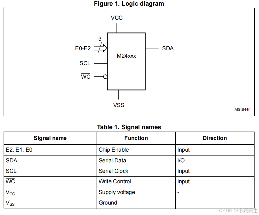
2 Signal description
2.1 Serial Clock (SCL)
The signal applied on the SCL input is used to strobe the data available on SDA(in) and to output the data on SDA(out).
应用在SCL输入上的信号用于检测SDA(in)上的可用数据,并在SDA上输出数据(输出)。
2.2 Serial Data (SDA)
SDA is an input/output used to transfer data in or data out of the device. SDA(out) is an open drain output that may be wire-OR’ed with other open drain or open collector signals on the bus. A pull-up resistor must be connected from Serial Data (SDA) to VCC (Figure 15 indicates how to calculate the value of the pull-up resistor).
SDA是一种输入/输出,用于传输设备中的数据或输出设备中的数据。SDA(输出)是一个开路漏极输出,可与母线上的其他开路漏极或开路集电极信号通过导线连接。上拉电阻必须从串行数据(SDA)连接到VCC(图15指示了如何计算上拉电阻的值)。
2.3 Chip Enable (E2, E1, E0)
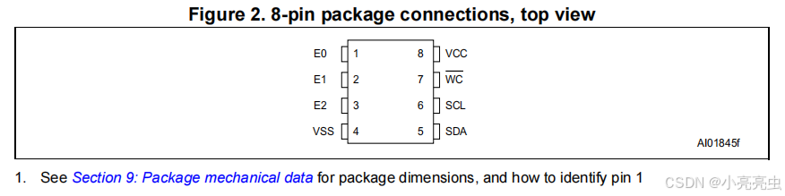
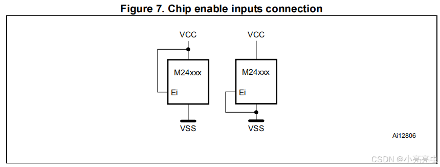
(E2,E1,E0) input signals are used to set the value that is to be looked for on the three least significant bits (b3, b2, b1) of the 7-bit device select code (see Table 3). These inputs must be tied to VCC or VSS, as shown in Figure 7. When not connected (left floating), these inputs are read as low (0).
(E2、E1、E0)输入信号用于设置要在7位设备选择代码的三个最小有效位(b3、b2、b1)上查找的值(见表3)。这些输入必须绑定到VCC或VSS,如图7所示。当未连接(左浮动)时,这些输入被读取为低(0)。
For the 4-balls WLCSP package (see Figure 4), the (E2,E1,E0) inputs are internally connected to (0, 0, 0).
对于4-ball WLCSP包(见图4),(E2、E1、E0)输入在内部连接到(0、0、0)。
For the 5-balls WLCSP package (see Figure 5), the (E2,E1,E0) inputs are internally connected to (0,0,1)
对于5-ball WLCSP软件包(参见图5),(E2、E1、E0)输入端内部连接到(0、0、1)。
2.4 Write Control (WC)
This input signal is useful for protecting the entire contents of the memory from inadvertent write operations. Write operations are disabled to the entire memory array when Write Control (WC) is driven high. Write operations are enabled when Write Control (WC) is either driven low or left floating.
这个输入信号对于保护内存的整个内容不受无意的写操作非常有用。当写控制(WC)驱动高时,禁用整个内存阵列的写操作。当写入控制(WC)低驱动或保持浮动时,启用写入操作。
When Write Control (WC) is driven high, device select and address bytes are acknowledged, Data bytes are not acknowledged.
当写入控制(WC)驱动到高时,确认设备选择和地址字节,数据字节不确认。
2.5 VSS (ground)
VSS is the reference for the VCC supply voltage.
VSS是VCC电源电压的参考
2.6 Supply voltage (VCC)
2.6.1 Operating supply voltage (VCC)
Prior to selecting the memory and issuing instructions to it, a valid and stable VCC voltage within the specified [VCC(min), VCC(max)] range must be applied (see Operating conditions in Section 8: DC and AC parameters). In order to secure a stable DC supply voltage, it is recommended to decouple the VCC line with a suitable capacitor (usually of the order of 10 nF to 100 nF) close to the VCC/VSS package pins.
在选择内存并向其发出指令之前,必须在指定的[VCC(最小),VCC(最大)]范围内施加有效且稳定的VCC电压(参见第8节中的操作条件:直流和交流参数)。为了确保稳定的直流电源电压,建议使用靠近VCC/VSS封装引脚的合适电容器(通常为10 nF到100 nF)将VCC线路解耦。
This voltage must remain stable and valid until the end of the transmission of the instruction and, for a write instruction, until the completion of the internal write cycle (tW).
该电压必须保持稳定和有效,直到指令传输结束,对于写入指令,直到内部写入周期(tW)完成。
2.6.2 Power-up conditions
The VCC voltage has to rise continuously from 0 V up to the minimum VCC operating voltage (see Operating conditions in Section 8: DC and AC parameters).
VCC电压必须从0V持续上升至最小VCC工作电压(参见第8节中的工作条件:直流和交流参数)。
2.6.3 Device reset
In order to prevent inadvertent write operations during power-up, a power-on-reset (POR) circuit is included.
为了防止在通电过程中无意的写入操作,包括电源复位(POR)电路。
At power-up, the device does not respond to any instruction until VCC has reached the internal reset threshold voltage. This threshold is lower than the minimum VCC operating voltage (see Operating conditions in Section 8: DC and AC parameters). When VCC passes over the POR threshold, the device is reset and enters the Standby Power mode; however, the device must not be accessed until VCC reaches a valid and stable DC voltage within the specified [VCC(min), VCC(max)] range (see Operating conditions in Section 8: DC and AC parameters).
在通电时,直到VCC达到内部复位阈值电压之前,设备不会响应任何指令。该阈值低于最小VCC工作电压(参见第8节中的工作条件:直流和交流参数)。当VCC超过POR阈值时,设备复位并进入备用电源模式;但是,直到VCC达到规定的[VCC(最小),VCC(最大)]范围内有效和稳定的直流电压)(参见第8节:直流和交流参数)。
In a similar way, during power-down (continuous decrease in VCC), the device must not be accessed when VCC drops below VCC(min). When VCC drops below the power-on-reset threshold voltage, the device stops responding to any instruction sent to it.
同样,在断电期间(VCC持续下降),当VCC低于VCC(min)时,不能访问设备。当VCC低于电源复位阈值电压时,设备停止响应发送给它的任何指令。
2.6.4 Power-down conditions
During power-down (continuous decrease in VCC), the device must be in the Standby Power mode (mode reached after decoding a Stop condition, assuming that there is no internal write cycle in progress).
在断电期间(VCC持续下降),设备必须处于待机电源模式(假设没有正在进行的内部写入循环,解码停止条件后达到的模式)。
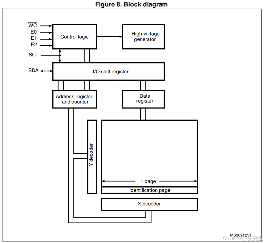
3 Memory organization
The memory is organized as shown below.
4 Device operation
The device supports the I2C protocol. This is summarized in Figure 9. Any device that sends data on to the bus is defined to be a transmitter, and any device that reads the data to be a receiver. The device that controls the data transfer is known as the bus master, and the other as the slave device. A data transfer can only be initiated by the bus master, which will also provide the serial clock for synchronization. The device is always a slave in all communications
该设备支持I2C协议。图9总结了这一点。向总线发送数据的任何设备都被定义为发射器,而读取数据的任何设备都被定义为接收器。控制数据传输的设备称为总线主设备,另一个称为从设备。数据传输只能由总线主服务器发起,它也将为同步提供串行时钟。(new add:这款芯片)该设备在所有通信中都始终是一个从属设备。
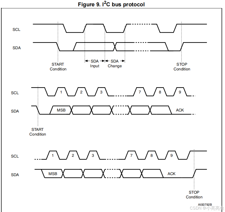
4.1 Start condition
Start is identified by a falling edge of Serial Data (SDA) while Serial Clock (SCL) is stable in the high state. A Start condition must precede any data transfer instruction. The device continuously monitors (except during a Write cycle) Serial Data (SDA) and Serial Clock (SCL) for a Start condition.
启动由串行数据(SDA)的下降边标识,而串行时钟(SCL)在高状态下保持稳定。启动条件必须出现在任何数据传输指令之前。设备持续监控(在写入周期中除外)串行数据(SDA)和串行时钟(SCL)的启动条件。
4.2 Stop condition
Stop is identified by a rising edge of Serial Data (SDA) while Serial Clock (SCL) is stable and driven high. A Stop condition terminates communication between the device and the bus master. A Read instruction that is followed by NoAck can be followed by a Stop condition to force the device into the Standby mode.
停止由串行数据(SDA)的上升边缘标识,而串行时钟(SCL)则稳定且驱动值较高。停止条件终止设备与总线主机之间的通信。在NoAck之后的读取指令可以遵循一个停止条件来强制设备进入待机模式。
A Stop condition at the end of a Write instruction triggers the internal Write cycle.
写指令结束时的停止条件会触发内部写循环。
4.3 Data input
During data input, the device samples Serial Data (SDA) on the rising edge of Serial Clock (SCL). For correct device operation, Serial Data (SDA) must be stable during the rising edge of Serial Clock (SCL), and the Serial Data (SDA) signal must change only when Serial Clock (SCL) is driven low.
在数据输入过程中,设备在串行时钟(SCL)的上升边缘上对串行数据(SDA)进行采样。为了进行正确的设备操作,在串行时钟(SCL)上升边缘时,串行数据(SDA)必须稳定,并且只有当串行时钟(SCL)驱动到较低时,串行数据(SDA)信号才必须改变。
4.4 Acknowledge bit (ACK)
The acknowledge bit is used to indicate a successful byte transfer. The bus transmitter, whether it be bus master or slave device, releases Serial Data (SDA) after sending eight bits of data. During the 9th clock pulse period, the receiver pulls Serial Data (SDA) low to acknowledge the receipt of the eight data bits.
确认位用于表示一个成功的字节转移。总线发射机,无论是总线主设备还是从设备,都会在发送8位数据后释放串行数据(SDA)。在第9个时钟脉冲周期期间,接收机将串行数据(SDA)拉到低,以确认接收到8个数据位。
4.5 Device addressing
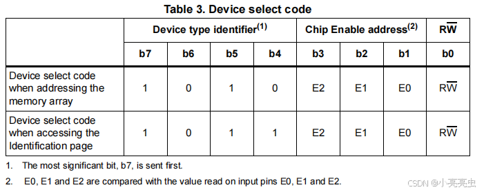
To start communication between the bus master and the slave device, the bus master must initiate a Start condition. Following this, the bus master sends the device select code, shown in Table 3 (most significant bit first).
要启动总线主设备和从属设备之间的通信,总线主机必须启动一个启动条件。随后,总线主设备发送设备选择代码,如表3所示(最重要的位)。
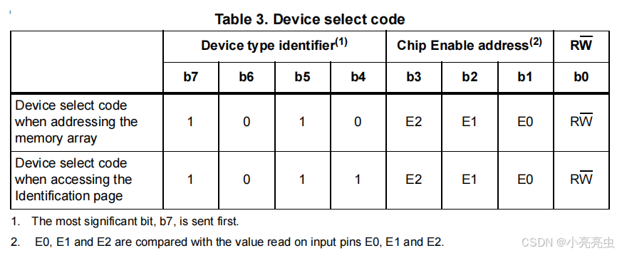
When the device select code is received, the device only responds if the Chip Enable address is the same as the value on its Chip Enable E2,E1,E0 inputs.
当接收到设备选择代码时,只有当芯片启用地址与其芯片启用E2、E1、E0输入上的值相同时,设备才会响应。
The 8th bit is the Read/Write bit (RW). This bit is set to 1 for Read and 0 for Write operations.
第8位是读/写位(RW)。读操作设置为1,写操作设置为0。
If a match occurs on the device select code, the corresponding device gives an acknowledgment on Serial Data (SDA) during the 9th bit time. If the device does not match the device select code, the device deselects itself from the bus, and goes into Standby mode.
如果在设备选择代码上发生匹配,则相应的设备将在第9位时间内对串行数据(SDA)进行确认。如果设备与设备选择代码不匹配,则设备将从总线上取消选择自己,并进入待机模式。
5 Instructions
5.1 Write operations
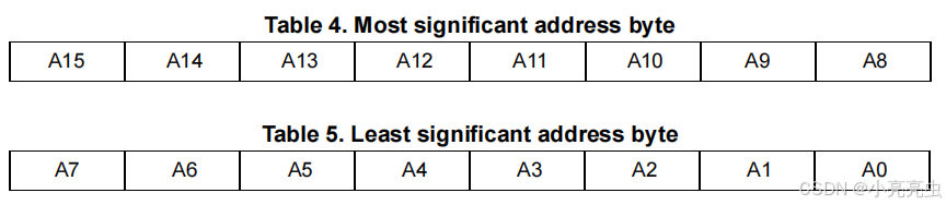
Following a Start condition the bus master sends a device select code with the R/W bit (RW) reset to 0. The device acknowledges this, as shown in Figure 10, and waits for two address bytes. The device responds to each address byte with an acknowledge bit, and then waits for the data byte.
根据启动条件,总线主机发送设备选择代码,R/W位(RW)重置为0。设备承认这一点,如图10所示,并等待两个地址字节。该设备用一个确认位响应每个地址字节,然后等待该数据字节。
When the bus master generates a Stop condition immediately after a data byte Ack bit (in the “10th bit” time slot), either at the end of a Byte Write or a Page Write, the internal Write cycle tW is triggered. A Stop condition at any other time slot does not trigger the internal Write cycle.
当总线主节点在数据字节Ack位(在“第10位”时间隙中)之后立即生成停止条件时,无论是在字节写还是页面写结束时,都会触发内部写循环tW。任何其他时间槽中的停止条件都不会触发内部写入循环。
After the Stop condition and the successful completion of an internal Write cycle (tW), the device internal address counter is automatically incremented to point to the next byte after the last modified byte.
在“停止”条件并成功完成内部写入周期(tW)后,设备内部地址计数器将自动递增,以指向最后一个修改字节之后的下一个字节。
During the internal Write cycle, Serial Data (SDA) is disabled internally, and the device does not respond to any requests.
在内部写入周期中,串行数据(SDA)在内部被禁用,并且设备不响应任何请求。
If the Write Control input (WC) is driven High, the Write instruction is not executed and the accompanying data bytes are not acknowledged, as shown in Figure 11.
如果写入控制输入(WC)被驱动为高,则不执行写入指令,伴随的数据字节不被确认,如图11所示。
5.1.1 Byte Write
After the device select code and the address bytes, the bus master sends one data byte. If the addressed location is Write-protected, by Write Control (WC) being driven high, the device replies with NoAck, and the location is not modified. If, instead, the addressed location is not Write-protected, the device replies with Ack. The bus master terminates the transfer by generating a Stop condition, as shown in Figure 10.
在设备选择代码和地址字节后,总线主机发送一个数据字节。如果寻址位置是写保护,由写控制(WC)被驱动高,设备用NoAck回复,位置不修改。如果寻址位置没有写保护,设备会用Ack回复。总线主线通过生成停止条件来终止传输,如图10所示。
5.1.2 Page Write
The Page Write mode allows up to 32 byte to be written in a single Write cycle, provided that they are all located in the same page in the memory: that is, the most significant memory address bits, A15/A5, are the same. If more bytes are sent than will fit up to the end of the page, a “roll-over” occurs, i.e. the bytes exceeding the page end are written on the same page, from location 0.
页面写入模式允许在单个写入周期中写入多达32个字节,只要它们都位于内存中的同一页面中:即,最重要的内存地址位A15/A5是相同的(注解:1.A15和A5来源于Table 4. Most significant address byte,里面地址位的标识。 2."A15/A"表示的是A5位到A15位。 3.A0到A4表示的是一页里面的地址,A5到A15表示的是不同的页的起始地址)。如果发送的字节超过了页面的结尾,就会发生“滚动”,即超过页面结尾的字节从位置0写在同一页面上。
The bus master sends from 1 to 32 byte of data, each of which is acknowledged by the device if Write Control (WC) is low. If Write Control (WC) is high, the contents of the addressed memory location are not modified, and each data byte is followed by a NoAck, as shown in Figure 11. After each transferred byte, the internal page address counter is incremented.
总线主服务器发送从1到32字节的数据,如果写控制(WC)是低,每个数据都由设备确认。如果写控制(WC)是高,则不会修改寻址内存位置的内容,每个数据字节后面都有一个NoAck,如图11所示。在每个传输的字节之后,内部页面地址计数器将会递增。
The transfer is terminated by the bus master generating a Stop condition.
传输由总线主机产生一个停止条件而终止。
5.1.3 Write Identification Page (M24C64-D only)
The Identification Page (32 byte) is an additional page which can be written and (later) permanently locked in Read-only mode. It is written by issuing the Write Identification Page instruction. This instruction uses the same protocol and format as Page Write (into memory array), except for the following differences:
标识页面(32字节)是一个附加页面,可以写入并(稍后)永久锁定在只读模式下。它是通过发出写识别页指令来编写的。此指令使用与“页面写入”(进入内存数组)相同的协议和格式,但存在以下差异:
• Device type identifier = 1011b
• MSB address bits A15/A5 are don’t care except for address bit A10 which must be ‘0’.
LSB address bits A4/A0 define the byte address inside the Identification page.
设备类型标识符= 1011b
MSB地址位A15/A5并不关心,除了地址位A10必须是“0”。("地址位A10必须是“0”"不懂为什么)
LSB地址位A4/A0定义了标识页面内的字节地址。(1page=32byte, 0x00~0x1F就可以表示)
If the Identification page is locked, the data bytes transferred during the Write Identification Page instruction are not acknowledged (NoAck).
如果标识页面被锁定,则在写识别页面指令期间传输的数据字节不会被确认(NoAck)。
5.1.4 Lock Identification Page (M24C64-D only)
The Lock Identification Page instruction (Lock ID) permanently locks the Identification page in Read-only mode. The Lock ID instruction is similar to Byte Write (into memory array) with the following specific conditions:
锁定标识页指令(锁定ID)永久锁定在只读模式。锁ID指令类似于“字节写入”(进入内存数组),具体条件如下:
• Device type identifier = 1011b
• Address bit A10 must be ‘1’; all other address bits are don’t care
• The data byte must be equal to the binary value xxxx xx1x, where x is don’t care
设备类型标识符= 1011b
地址位A10必须是“1”;所有其他地址位都不关心
数据字节必须等于二进制值xxxx xx1x,其中x并不关心
5.1.5 ECC (Error Correction Code) and Write cycling
The ECC is offered only in devices identified with process letter K, all other devices (identified with a different process letter) do not embed the ECC logic.
ECC仅可在标识有工艺字母K的设备中提供,所有其他设备(用不同的工艺字母标识)不嵌入ECC逻辑。
The Error Correction Code (ECC) is an internal logic function which is transparent for the I2C communication protocol.
纠错码(ECC)是一个内部逻辑功能,对I 2C通信协议是透明的。
The ECC logic is implemented on each group of four EEPROM bytes(1). Inside a group, if a single bit out of the four bytes happens to be erroneous during a Read operation, the ECC detects this bit and replaces it with the correct value. The read reliability is therefore much improved.
ECC逻辑在每一组四个EEPROM字节(1)上实现的。在组内部,如果在读取操作中四个字节中的一个位恰好错误,ECC会检测到这个位并用正确的值替换它。因此,读取的可靠性被大大提高了。
Even if the ECC function is performed on groups of four bytes, a single byte can be written/cycled independently. In this case, the ECC function also writes/cycles the three other bytes located in the same group(1). As a consequence, the maximum cycling budget is defined at group level and the cycling can be distributed over the 4 bytes of the group: the sum of the cycles seen by byte0, byte1, byte2 and byte3 of the same group must remain below the maximum value defined Table 12: Cycling performance.
即使ECC函数是在四个字节的组上执行的,也可以独立地写入/循环单个字节。在这种情况下,ECC函数还会写入/循环位于同一组(1)中的其他三个字节。因此,在组级别定义最大循环预算,循环可以分布在组的4字节上:同一组的字节0、字节1、字节2和字节3的循环总和必须低于表12定义的最大值:循环性能。
5.1.6 Minimizing Write delays by polling on ACK
During the internal Write cycle, the device disconnects itself from the bus, and writes a copy of the data from its internal latches to the memory cells. The maximum Write time (tw) is shown in AC characteristics tables in Section 8: DC and AC parameters, but the typical time is shorter. To make use of this, a polling sequence can be used by the bus master.
在内部写周期中,设备断开自己与总线的连接,并将数据的副本从其内部锁存器写入内存单元。最大写入时间(tw)显示在第8节的交流特性表中:直流和交流参数,但典型的时间较短。为了利用这一点,总线主服务器可以使用轮询序列。
The sequence, as shown in Figure 12, is:
如图12所示,其顺序为:
• Initial condition: a Write cycle is in progress.
• Step 1: the bus master issues a Start condition followed by a device select code (the first byte of the new instruction).
• Step 2: if the device is busy with the internal Write cycle, no Ack will be returned and the bus master goes back to Step 1. If the device has terminated the internal Write cycle, it responds with an Ack, indicating that the device is ready to receive the second part of the instruction (the first byte of this instruction having been sent during Step 1)
初始条件:写入循环正在进行中。
•步骤1:总线主机发出一个启动条件,然后是一个设备选择代码(新指令的第一个字节)。
•步骤2:如果设备忙于内部写入周期,则不会返回Ack,总线主机返回到步骤1。如果设备已经终止了内部写入周期,它用Ack响应,表明设备已经准备好接收指令的第二部分(该指令的第一个字节在步骤1中已经发送)。
5.2 Read operations
Read operations are performed independently of the state of the Write Control (WC) signal.
读取操作将独立于写控制(WC)信号的状态来执行。
After the successful completion of a Read operation, the device internal address counter is incremented by one, to point to the next byte address.
成功完成读取操作后,设备内部地址计数器增加1,以指向下一个字节地址。
For the Read instructions, after each byte read (data out), the device waits for an acknowledgment (data in) during the 9th bit time. If the bus master does not acknowledge during this 9th time, the device terminates the data transfer and switches to its Standby mode.
对于读取指令,在每个字节读取(数据输出)之后,设备将在第9位时间内等待确认(数据输入)。如果总线主线在第9次不承认,设备终止数据传输并切换到待机模式。

5.2.1 Random Address Read
A dummy Write is first performed to load the address into this address counter (as shown in Figure 13) but without sending a Stop condition. Then, the bus master sends another Start condition, and repeats the device select code, with the RW bit set to 1. The device acknowledges this, and outputs the contents of the addressed byte. The bus master must not acknowledge the byte, and terminates the transfer with a Stop condition.
首先执行虚拟写入,以将地址加载到此地址计数器中(如图13所示),但不发送停止条件。然后,总线主服务器发送另一个开始条件,并重复设备选择代码,将RW位设置为1。设备承认这一点,并输出被寻址字节的内容。总线主节点不能承认该字节,并以停止条件终止传输。
5.2.2 Current Address Read
For the Current Address Read operation, following a Start condition, the bus master only sends a device select code with the R/W bit set to 1. The device acknowledges this, and outputs the byte addressed by the internal address counter. The counter is then incremented. The bus master terminates the transfer with a Stop condition, as shown in Figure 13, without acknowledging the byte.
对于当前地址读取操作,根据启动条件,总线主机只发送一个将R/W位设置为1的设备选择代码。设备承认这一点,并输出由内部地址计数器寻址的字节。然后再增加该计数器。总线主服务器以停止条件终止传输,如图13所示,而不确认字节
Note that the address counter value is defined by instructions accessing either the memory or the Identification page. When accessing the Identification page, the address counter value is loaded with the byte location in the Identification page, therefore the next Current Address Read in the memory uses this new address counter value. When accessing the memory, it is safer to always use the Random Address Read instruction (this instruction loads the address counter with the byte location to read in the memory, see Section 5.2.1) instead of the Current Address Read instruction.
请注意,地址计数器的值是由访问内存或标识页面的指令定义的。当访问标识页面时,地址计数器值与标识页面中的字节位置一起加载,因此内存中的下一个当前地址读取使用这个新的地址计数器值。在访问内存时,始终使用随机地址读指令(该指令加载地址计数器的字节位置,见第5.2.1节)而不是当前地址读指令更安全。
5.2.3 Sequential Read
This operation can be used after a Current Address Read or a Random Address Read. The bus master does acknowledge the data byte output, and sends additional clock pulses so that the device continues to output the next byte in sequence. To terminate the stream of bytes, the bus master must not acknowledge the last byte, and must generate a Stop condition, as shown in Figure 13.
此操作可以在当前地址读取或随机地址读取之后使用。总线主服务器确实承认数据字节的输出,并发送额外的时钟脉冲,以便设备继续按顺序输出下一个字节。要终止字节流,总线主机不能确认最后一个字节,并且必须生成一个停止条件,如图13所示。
The output data comes from consecutive addresses, with the internal address counter automatically incremented after each byte output. After the last memory address, the address counter “rolls-over”, and the device continues to output data from memory address 00h.
输出数据来自连续的地址,内部地址计数器在每个字节输出后自动递增。在最后一个内存地址之后,地址计数器“滚转”,设备继续从内存地址00h输出数据。
5.3 Read Identification Page (M24C64-D only)
The Identification Page (32 bytes) is an additional page which can be written and (later) permanently locked in Read-only mode.
标识页面(32字节)是一个附加页面,可以写入并(稍后)永久锁定在只读模式下。
The Identification Page can be read by issuing an Read Identification Page instruction. This instruction uses the same protocol and format as the Random Address Read (from memory array) with device type identifier defined as 1011b. The MSB address bits A15/A5 are don’t care, the LSB address bits A4/A0 define the byte address inside the Identification Page. The number of bytes to read in the ID page must not exceed the page boundary (e.g.: when reading the Identification Page from location 10d, the number of bytes should be less than or equal to 22, as the ID page boundary is 32 bytes).
可以通过发出读取识别页面指令来阅读识别页面。该指令使用与随机地址读取(从内存数组)相同的协议和格式,设备类型标识符定义为1011b。MSB地址位A15/A5并不在乎,LSB地址位A4/A0定义了标识页面内的字节地址。要在ID页面中读取的字节数不能超过页面边界。:当从位置10d读取标识页面时,字节数应小于或等于22,因为ID页面边界为32字节)。
5.4 Read the lock status (M24C64-D only)
The locked/unlocked status of the Identification page can be checked by transmitting a specific truncated command [Identification Page Write instruction + one data byte] to the device. The device returns an acknowledge bit if the Identification page is unlocked, otherwise a NoAck bit if the Identification page is locked.
可以通过将一个特定的截断命令[识别页面写指令+一个数据字节]传输到设备,来检查识别页面的锁定/解锁状态。如果标识页面被解锁,设备返回一个确认位,否则如果标识页面被锁定,则返回一个NoAck位。
Right after this, it is recommended to transmit to the device a Start condition followed by a Stop condition, so that:
在此之后,建议立即向设备发送启动条件和停止条件,以便:
• Start: the truncated command is not executed because the Start condition resets the device internal logic,
• Stop: the device is then set back into Standby mode by the Stop condition.
启动:未执行,因为开始条件重置设备内部逻辑,
停止:然后通过停止条件将设备设置为待机模式。
6 Initial delivery state
初始交付状态
The device is delivered with all the memory array bits and Identification page bits set to 1 (each byte contains FFh).
设备将所有内存阵列位和识别页面位设置为1(每个字节包含FFh)。
When delivered in unsawn wafer, all memory bits are set to 1 (each memory byte contains FFh) except the last byte located at address 1FFFh which is written with the value 22h
当在未售出的晶圆中交付时,所有存储位都设置为1(每个存储字节包含FFh),但位于地址1FFFh的最后一个字节除外,该字节的值为22h
7.Code
(待验证,再补上)


 563
563

 被折叠的 条评论
为什么被折叠?
被折叠的 条评论
为什么被折叠?
 到【灌水乐园】发言


