


1.上篇的一个尾巴,不解释了
8:
    TTYDBG("LS3A-7A linkup.")    //HT链接建立
//setup LS3A - 7A HT link done.

    bal  beep_off
    nop
2.正式开始,继续读代码
    TTYDBG("\r\nStart Init Memory, wait a while......\r\n")         //内存控制器初始化
####################################
    move    msize, $0
    move    s3, $0
//!!!!important--s1 must be correctly set

    TTYDBG("NODE 0 MEMORY CONFIG BEGIN\r\n")
重点来了,要开始初始化内存了,难,我估计我看不很懂。
两个寄存器赋初值0. msize 是s2
2.1 看一眼原理图,内存相关的部分。

原理图太多,MC0和MC1 都连接了这样的内存芯片,每个控制器连接8片,共16片

暂时没有找到相关pdf,从百度上看,8Gbits(1GB),16位宽,ddr3类型。
每个通道是8GB ,总共内存大小16GB
3.继续读代码
    //set MC1 dimm infor
    dli     a0, ( MC_SDRAM_TYPE_DDR3    /* sdram type: DDR3/DDR2 */ \
                | MC_DIMM_ECC_NO        /* dimm ECC: YES/NO */ \
                | MC_DIMM_BUF_REG_NO    /* dimm buffer register: YES/NO, for RDIMM use YES, all else use NO*/ \
                | MC_DIMM_WIDTH_64      /* memory data width: 64/32 */ \
                | MC_SDRAM_ROW_16       /* sdram row address number: 15~11 */ \
                | MC_SDRAM_COL_10       /* sdram column address number: 12~9 */ \
                | MC_SDRAM_BANK_8       /* sdram bank number: 8/4 */ \
                | MC_ADDR_MIRROR_NO    /* for standard DDR3 UDIMM, use YES else use NO */ \
                | MC_SDRAM_WIDTH_X16    /* SDRAM device data width: 8/16 */ \
                | MC_USE_CS_0_1         /* the CS pins the sdram connected on(split by '_', from small to big) */ \
                | MC_MEMSIZE_(16)        /* MC memory size, unit: 512MB */ \
                )
    dsll    s1, a0, 32
    //set MC0 dimm infor
    dli     a0, ( MC_SDRAM_TYPE_DDR3    /* sdram type: DDR3/DDR2 */ \
                | MC_DIMM_ECC_NO        /* dimm ECC: YES/NO */ \
                | MC_DIMM_BUF_REG_NO    /* dimm buffer register: YES/NO, for RDIMM use YES, all else use NO*/ \
                | MC_DIMM_WIDTH_64      /* memory data width: 64/32 */ \
                | MC_SDRAM_ROW_16       /* sdram row address number: 15~11 */ \
                | MC_SDRAM_COL_10       /* sdram column address number: 12~9 */ \
                | MC_SDRAM_BANK_8       /* sdram bank number: 8/4 */ \
                | MC_ADDR_MIRROR_NO    /* for standard DDR3 UDIMM, use YES, else use NO */ \
                | MC_SDRAM_WIDTH_X16    /* SDRAM device data width: 8/16 */ \
                | MC_USE_CS_0_1         /* the CS pins the sdram connected on(split by '_', from small to big) */ \
                | MC_MEMSIZE_(16)        /* MC memory size, unit: 512MB 512*16共8G */ \
                )
    or      s1, s1, a0      //内存初始化参数,高32位,低32位一样
    //set used MC and NODE ID
    or      s1, s1, USE_MC_0_1          /* used memory controller: _0/_1/_0_1 */
    or      s1, s1, MC_NODE_ID_0        /* node ID: 0/1/2/3 */
准备参数。MC0和MC1两个控制器都有设置。设置的内容基本相同。
主要保存在s1寄存器中了。
4. 继续,又来了一个包含语句
#include "ddr_dir/loongson3A2000_ddr2_config.S"
4.1 这时候,程序要运行到这个文件的代码了。
/**********************************
loongson3A2000_ddr2_config.S
used to set up ddr controllers MC0 and MC1 //用于设置DDR控制器MC0,MC1
and set up the memory space on L2 Xbar //设置L2XBAR
input: s1--MC1 & MC0 DIMM info and Node ID //输入参数
note: s1 is damaged by the end of this file //注意,s1被损坏,在这个文件结束的时候
original: whd
rewrite by Chen Xinke on 11/11/2010
1: reorder the program
2: DIMM info and memory size is set according to s1[MC1&0_MEMSIZE]
note: config L2 Xbar still need to be finished,currently only support limited MEMSIZE.
v1.0 raw
v1.2 add support for 4G memsize per MC, modify the L2-Xbar config manner of MC1
to reduce code size.
v1.4 Modify L2 Xbar config reg code at Interleave mode to reduce code size
new code:
1. according to Memsize config open space
2. config interleave bits
v1.6 Modify L2 Xbar address window configuration to new pmon-kernel interface.
(default use NO_INTERLEAVE)
v1.8 Modify supported Interleave bit. Add Interleave support when each MC uses 1GB or 2GB.
v2.0 Add support for 8GB per MC.
v2.1 support for interleave using the X2 interleave function for 3A2000
************************************/
来点注释看一下。。。
4.2 检查需要初始化的控制器
//make sure s1[3:2] is correctly set.          //开始执行
    GET_MC_SEL_BITS             //[3:2] 表示MC1,MC0 0表示两个控制器都有效
    dli     a2, 3
    bne     a1, a2, 1f         //不等于3,则跳转
    nop
//s1[3:2]=0b'11, clear to 0b'00
    dli     a2, 0xc
    not     a2, a2
    and     s1, s1, a2         //等于3,则清零[3:2]位
1:
我们的代码实际是0,表示两个控制器都要设置。
4.3 还有一段注释,还是可以留意以下
/**************************
1. 1. check NODE memory size. //检查内存大小
* 2. set MC0/1_ONLY if the following 2 conditions are satisfied: //如果以下两个条件满足,设置MC0/1_ONLY
* (1). s1[3:2]=0b'00
* (2). MC0 or MC1 MEMSIZE > 0.
* when use AUTO_DDR_CONFIG, one MC may have no DIMM while the other has, in this case,
* the code should set MC0_ONLY or MC1_ONLY in s1 automatically, because the code of
* configuring L2-Xbar will use this message.
**************************/
4.4 检查内存大小
    GET_MC0_ONLY
    bnez    a1, 1f   //不等于0跳转,实际等于0
    nop
    GET_MC1_ONLY
    bnez    a1, 2f   //不等于0跳转,实际等于0
    nop
//s1[3:2]=0b'00
    //check memory size in this case
    GET_MC0_MEMSIZE   //获得控制器0的内存大小 8G ,得16
    move    t5, a1
    GET_MC1_MEMSIZE   //获得控制器0的内存大小 8G ,得16
    daddu   a1, a1, t5   //a1= 32,共16G
    beqz    a1, 89f    //等于0跳转,实际不跳转
    nop
    dli     t5, 0x20
    bgt     a1, t5, 89f  //大于32跳转89,实际不大于
    nop
    GET_MC0_MEMSIZE    //得16,a1=16
    bnez    a1, 3f     //不等于0,跳转
    nop
    //MC0_MEMSIZE=0, MC1_MEMSIZE must !=0, set MC1_ONLY ,被跳过
    dli     t5, 0x8
    or      s1, t5     //[3] = 1
    b       4f
    nop
3:  //MC0_MEMSIZE!=0
    GET_MC1_MEMSIZE   //得16,a1=16
    bnez    a1, 4f    //不等于0,跳转
    nop
    //MC1_MEMSIZE=0 set use MC0_ONLY
    dli     t5, 0x4
    or      s1, t5
    b       4f
    nop
1:  //MC0_ONLY
    GET_MC0_MEMSIZE
    b       5f
    nop
2:  //MC1_ONLY
    GET_MC1_MEMSIZE
5:
    beqz    a1, 89f
    nop
    dli     t5, 0x10
    bgt     a1, t5, 89f
    nop
4:                           //继续执行
有几个标号是宏定义,暂不贴出来。正常时跳转到标号4继续执行。
4.5 设置控制器啦
/************************
2. set up Memory Controller.
************************/
/***********************
for single chip or multi-chip: //用于单芯片或者多芯片
t0: X-bar config base //xbar配置基地址
t2: chip configuration register location //芯片的配置寄存器地址
t0,t2 shouldn't be changed to the end of this file. //这个文件结束时,t0
**********************/
4.6 设置控制器代码部分
    GET_NODE_ID_a0    //ddr_config_define.h 215行,得到node的值,当前为0,存在第44位。
    dli     t2, 0x900000001fe00180
    dli     t0, 0x900000003ff00000
    or      t2, t2, a0
    or      t0, t0, a0      //因为NODE是0,还是和原来的值一样

#if 1 // AdonWang disable cpu buffered read
/* !!!!!!!!!!!!! IMPORTANT !!!!!!!!!!!! */
    PRINTSTR("Disable cpu buffered read\r\n")    //打印
    lw      a1, 0x0(t2)
    li      a0, 0xfffffdff
    and     a1, a1, a0     //清零位[9]    user1.pdf 29/170页,允许MC1 DDR配置空间
    sw      a1, 0x0(t2)
#endif
看到配置寄存器,是禁止MC1的配置空间被清零,那就是允许配置。
4.7 继续
#if 1 // AdonWang disable ddr3 readbuff
/*      May Affect the Performance     */
//This seems better for the spec2000
//if we enable ECC, this bit will be reset
    PRINTSTR("Disable read buffer\r\n")
    lw      a1, 0x4(t2)
    li      a0, 0x18
    or      a1, a1, a0
    sw      a1, 0x4(t2)   //[39:32] 是保留位???
#endif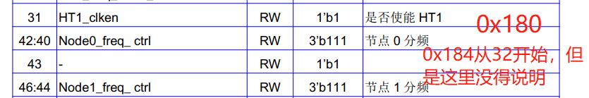
上图是0x180寄存器,从bit32开始是0x184的寄存器,但是文档中没有相关说明。
4.8 继续 ,看注释是要配置MC0了
//init MC1 will damage MC0 s1 info //初始化MC1,将损坏s1寄存器中MC0的部分的信息
//config MC0 if not define MC1_ONLY //配置MC0,如果没有定义MC1_ONLY
//-------------------------------------
4.9 继续看代码
10:
    GET_MC1_ONLY
    bnez    a1, 11f    //等于0,不跳转
    nop

    dli     t3, 0x0    //t3=0  , mc_init函数中用到。
#ifndef  DISABLE_DIMM_ECC   //宏被定义,代码不执行
    //Enable MC read buffer for ECC Initial
    GET_DIMM_ECC         //dimm ECC: NO  == 0
    beqz    a1, 8f       //等于0,跳转
    nop
    TTYDBG("Enable MC read buffer\r\n")
    lw      a1, 0x4(t2)
    li      a0, 0x8
    sll     a0, a0, t3
    not     a0, a0
    and     a1, a1, a0
    sw      a1, 0x4(t2)
    sync
8:
#endif
通过搜索,start.S中有这个宏定义。
这段代码中a1不等于0,不跳转,之后 t3 = 0;
4.10 继续看代码
	//start.S 1779行,包含ddr_dir/ls3A8_ddr_config.S,其中有mc_init
    bal     mc_init    //
    nop
跳转到一个函数执行。这个函数在ls3A8_ddr_config.S中,这个文件没有被显式编译,但是在start.S中被包含进来。(这种方式真的不太好阅读代码)

这个部分我觉得要先放一下,这里程序比较长,里面还有很多的函数跳转。先认为是一个MC的初始化吧。
这里两个参数,一个t7,为0,表示不自动训练参数,一个是t3 , 0--MC0; 1--MC1,这一次t3=0.
4.11 继续,这次初始化MC1
    PRINTSTR("\r\nMC0 Config DONE\r\n")
//-------------------------------------
//config MC1 if not define MC0_ONLY
11:
    GET_MC0_ONLY
    bnez    a1, 12f
    nop

    dli     t3, 0x1

    //shift MC1 DIMM info to low 32bit of s1
    dsrl    t5, s1, 32
    dli     a1, 0xffff8000
    and     t5, t5, a1
    dli     a1, 0xffffffff8000ffff
    and     s1, s1, a1
    or      s1, s1, t5
a1肯定不是0,不跳转,
t3 = 1 ,一会函数调用的参数。
s1右移32位后把值赋给t5
t5的值与操作0xffff,8000,剩下高17位。0-14被清零。
s1与操作0xffff,ffff,8000,ffff 在这MC0的配置信息被破坏了。MC0的信息只剩下高[31]位,和低[15:0]这17位有效了。
t5的值与s1的值或操作。
s1低32位中包含了一些MC1的信息。高32位不变
s1 的值原来是 3<<30|0<<29|0<<28|0<<27|0<<24|2<<20|1<<23|0<<22|1<<25|3<<16|16<<8
高32位与低32位相同。
其中[3:2] = 0,表示使用MC1和MC0
[0] = 0 表示NODE_ID = 0;
经过以上与或操作后。主要考虑的是MC1和MC0两个内存的大小一致。都是8G
S1 = 3<<30|0<<29|0<<28|0<<27|0<<24|2<<20|1<<23|0<<22|1<<25|3<<16|16<<8
4.12 参数准备好之后,就开始初始化这个控制器了。
    bal     mc_init
    nop
后面再分析吧。
4.13 初始化之后,配置xbar
    TTYDBG("\r\nMC1 Config DONE\r\n")
//-------------------------------------
12:
/*******************************
 3. config L2 X-bar
    code procedure: first, MC*_ONLY bits in s1 decides whether this MC is
    used,then according to MC*_MEMSIZE bits in s1 decide memory size and how
    the L2 X-bar windows will be configured.
    note: currently,when use only 1 MC,support memory size: 512M, 1G, 2G, 3G, 4G;
      when use MC0&MC1 both, only support 1G, 2G or 4G Memory size of each Controller.
*******************************/

    sync
    nop
    nop
    nop
    nop

    //disable default pci window
    L2XBAR_DISABLE_WINDOW(0x100);
注意一下注释。
宏定义展开:
#define L2XBAR_DISABLE_WINDOW(OFFSET) \
                        daddiu  v0, t0, OFFSET;       \
                        sd      $0, 0x80(v0);
t0 = 0x3ff0,0000,,访问的地址是0x3ff0,0180,PCI的基址设置为0.

,
4.14 继续看代码,设置xbar
    GET_MC_SEL_BITS
    beqz    a1, 1f    //a1等于0,跳转
    nop
1:
#ifndef NO_INTERLEAVE   //没定义,要执行
//interleave first, if MC1 memsize != MC0 memsize, do NO_interleave
    GET_MC0_MEMSIZE
    move    t5, a1        //a1= 16  (8G)
    GET_MC1_MEMSIZE
    bne     t5, a1, 1f     // 相等,不跳转
    nop
3:
    GET_NODE_ID_a0;       //a0 = 0 node_id
    XBAR_CONFIG_NODE_a0(0x10, \
                    0x0000000000000000, \
                    0xFFFFFFFFF0000000, \
                    0x00000000000000F0 | (MC_INTERLEAVE_OFFSET << 56))

    PRINTSTR("DDR Interleave space open : 0x00000000 - 0x0FFFFFFF\r\n")    //被打印
    b       2f
    nop
#endif

2:
    //Config PCI windows
    L2XBAR_CONFIG_PCI_AS_CPU(0x10);
    L2XBAR_CONFIG_PCI_BASE_0to8(0x110);
#ifndef NO_INTERLEAVE
    L2XBAR_CONFIG_PCI_AS_CPU(0x18);
    L2XBAR_CONFIG_PCI_BASE_0to8(0x118);
#endif
    PRINTSTR("PCI space open: 0x80000000 - 0x8FFFFFFF\r\n")
4.14.1 展开宏定义XBAR_CONFIG_NODE_a0
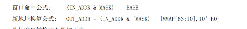
#define XBAR_CONFIG_NODE_a0(OFFSET, BASE, MASK, MMAP) \
                        daddiu  v0, t0, OFFSET;       \
                        dli     v1, BASE;             \
                        or      v1, v1, a0;           \
                        sd      v1, 0x00(v0);         \
                        dli     v1, MASK;             \
                        sd      v1, 0x40(v0);         \
                        dli     v1, MMAP;             \
                        sd      v1, 0x80(v0);
v0 = t0 + offset(0x10) = 0x900000003ff00010
v1 = 0,或上a0(0) 还是0
把v1(0) 写入 0x3ff0,0010
v1 = 0xffff,ffff,f000,000
把v1(0xffff,ffff,f000,000) 写入 0x3ff0,0050
v1 = 0x14000000000000F0
把v1(0x14000000000000F0) 写入 0x3ff0,0090

这里设置的是cpu_win2
base = 0;
mask= 0xffff,ffff,f000,000
mmap = 0x1400,0000,0000,00F0
mmap的低8位,低4位为0,指向DDR0,高4位为f,表示允许读和取指,并且使能映射。

高位[63:48] = 0x1400,转换后的仍然地址是0
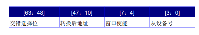
映射的区域0-0xfff,ffff。 映射out_addr 范围: 0x1400,0000,0000,0000~0x1400,0000,0fff,ffff
4.14.2 展开宏定义L2XBAR_CONFIG_PCI_AS_CPU
#define L2XBAR_CONFIG_PCI_AS_CPU(OFFSET) \
                        daddiu  v0, t0, OFFSET;       \
                        ld      v1, 0x0(v0);          \
                        sd      v1, 0x100(v0);        \
                        ld      v1, 0x40(v0);         \
                        sd      v1, 0x140(v0);        \
                        ld      v1, 0x80(v0);         \
                        sd      v1, 0x180(v0);
v0 = t0 + offset(0x10) = 0x900000003ff00010
v1 = 0x900000003ff00010寄存器的内容,
把v1 写入 0x3ff0,0110
v1 = 0x900000003ff00050寄存器的内容,
把v1写入 0x3ff0,0150
v1 = 0x900000003ff00090寄存器的内容
把v1写入 0x3ff0,0190
PCI win2的内容与CPUwin2的内容相同。
4.14.3 展开宏定义L2XBAR_CONFIG_PCI_BASE_0to8
#define L2XBAR_CONFIG_PCI_BASE_0to8(OFFSET) \
daddiu v0, t0, OFFSET; \
ld v1, 0x0(v0); \
dli a1, 0x80000000; \
or v1, v1, a1; \
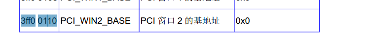
sd v1, 0x0(v0);v0 = t0 + offset(0x110) = 0x900000003ff00110
v1 = 0x900000003ff00110寄存器的内容。这个值是0
v1 或a1 = 0x8000,0000
PCI win2 base = 0x8000,0000
4.14.4 展开宏定义L2XBAR_CONFIG_PCI_AS_CPU
#define L2XBAR_CONFIG_PCI_AS_CPU(OFFSET) \
                        daddiu  v0, t0, OFFSET;       \
                        ld      v1, 0x0(v0);          \
                        sd      v1, 0x100(v0);        \
                        ld      v1, 0x40(v0);         \
                        sd      v1, 0x140(v0);        \
                        ld      v1, 0x80(v0);         \
                        sd      v1, 0x180(v0);
v0 = t0 + offset(0x18) = 0x900000003ff00018
读寄存器的内容到v1

这次是把CPUwin3的值,复制一份到PCI_WIN3的寄存器中。
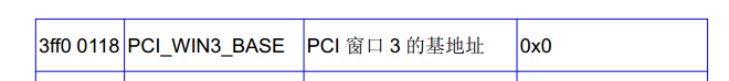
4.14.5 展开宏定义L2XBAR_CONFIG_PCI_BASE_0to8
#define L2XBAR_CONFIG_PCI_BASE_0to8(OFFSET) \
                        daddiu  v0, t0, OFFSET;       \
                        ld      v1, 0x0(v0);          \
                        dli     a1, 0x80000000;       \
                        or      v1, v1, a1;           \
                        sd      v1, 0x0(v0);
v0 = t0 + offset(0x118) = 0x900000003ff00118
v1 = 0x900000003ff00118寄存器的内容。这个值是0
v1 或a1 = 0x8000,0000
PCI win3 base = 0x8000,0000
明天继续吧。


 5835
5835


 被折叠的 条评论
为什么被折叠?
被折叠的 条评论
为什么被折叠?
 到【灌水乐园】发言


