


 本文深入剖析了Linux 3.10.52版本中SDIO设备的扫描步骤,包括设备接口、内部结构、命令与应答以及状态。通过对SDIO设备的初始化,如CMD5、CMD3、CMD8等命令的解析,揭示了设备的配置、状态转换和CIS信息的读取。文章特别强调了在不同状态和模式下命令的响应情况,以及数据线问题可能导致的初始化失败。
前言
本文基于Linux version 3.10.52版本代码分析sdio设备的扫描过程,同时选择sdio wifi设备作为分析对象,在分析过程中,附带上sdio的协议内容,帮助初学人员学习sdio协议基本内容及sdio的扫描过程。
1 SDIO设备接口及内部结构
本节介绍SDIO设备的硬件接口及内部寄存器等。
1.1 SDIO设备硬件接口
SDIO设备的硬件操作接口有3种方式:
A、 SPI mode;
B、 SD 1-bit mode;
C、 SD 4-bit mode;
这3种方式的硬件接口及管脚定义如下面图、表:
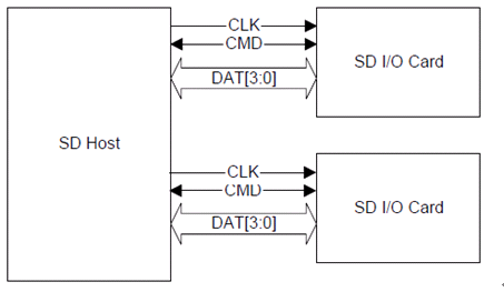
图1 SDIO硬件接口(连接了2组sdio设备)
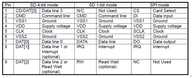
表1 SDIO各种模式管脚对应关系
本文不对SPI mode的相关内容介绍,有关SPI mode的内容不做过多说明。
1.2 SDIO设备内部寄存器
下图为SDIO设备内部操作空间的映射表。
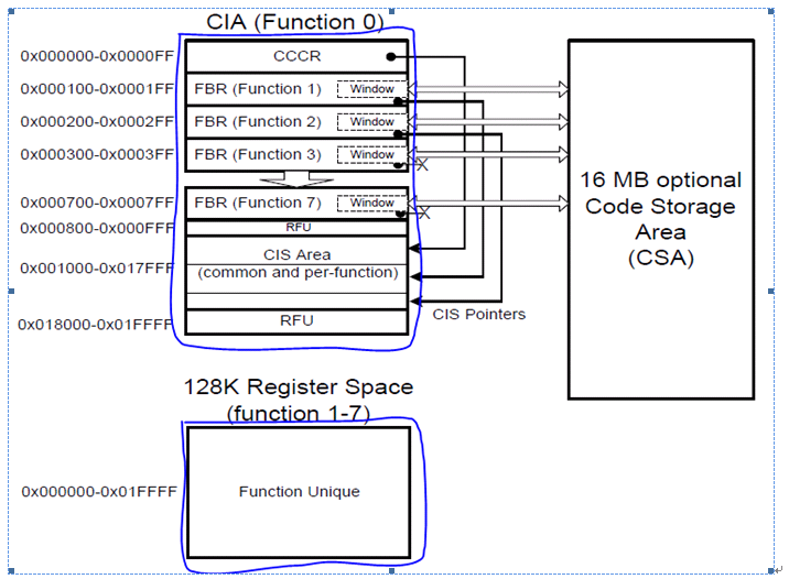
图2 sdio internal map
CIA: Common I/O Area
CCCR:Card Common Control Registers
FBR :Function Basic Registers
CIS:Card Information Structure
RFU: Reserved for Future Use
图中两个蓝色框表示的是一个东西,只是一个图更详细描述内部各个地址段的用途。CIS区域除了保存CIS信息外,sdio设备商也把设备使用的寄存器定义在这个区域,或作为RAM存储运行固件(fw)等。CSA区域的读写,需要借助FBR中的寄存器0xn0Ch—0xn0Eh、0xn0Fh(n等1~7)。
其中function number的个数随着不同设备而不同,并不一定都需要7个function,如后面介绍的扫描设备就只有function1、function2两个function。
CCCR、FBR、CIS区域的寄存器或数据存储格式如下面各个表,各个寄存器bit的意义在后面介绍扫描过程时再结合实际说明:
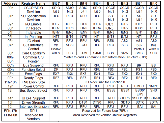
表2 Card Common Control Registers (CCCR)
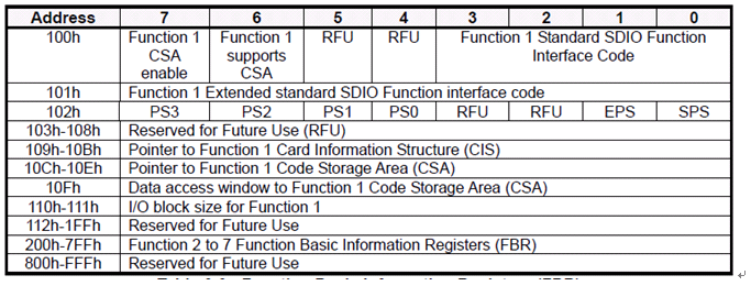
表3 Function Basic Information Registers (这里为function1的FBR)
在FBR寄存器中,0Ch—0Eh、0Fh用于读写CSA区域,操作方式如下面描述:
In order for the host to access a function’s CSA, it first shall determine if that function supports a CSA. The host reads the FBR register at address 00n00h where n is the function number (1 to 7). If bit 6=1, then the function supports a CSA and the host enables access by writing bit 7=1. The next step is for the host to load the 24 bit address to start reading or writing. This is accomplished by writing the 24 bits (A23-0) to registers
00n0Ch to 00n0Eh where n is the function number (1 to 7). Once the start address is written, data can be read or written by accessing register 00n0Fh, the CSA data window register. If more than 1 byte needs to be read or written, an extended I/O command (byte or block) can be performed with an OP code of 0 (fixed address). The address pointer shall be automatically incremented with each access to the window register, so the access will be to sequential addresses within the CSA. Once the operation is complete, the address of the NEXT operation shall be held in the 24 bit address register for the host to read.
CIS区域从0x001000h~0x017FFFh,其中CIS信息采用一种结构化的信息存储,每一条信息作为一个tuple结构体,该结构体中第一个字节为tuple code,用于表示该tuple存储的信息类型,第二个字节表示该tuple的长度n,同时也指明下一个tuple的开始位置,跟在长度后面就是n bytes的tuple内容,如下表所示。整个CIS信息最后是以一个0xFF字节作为结束符。
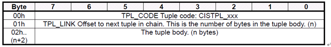
表4 Basic Tuple Format
SDIO支持的tuple code如下表:
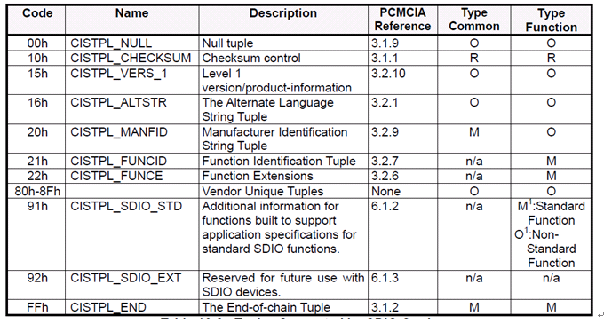
表5 Tuples Supported by SDIO Cards
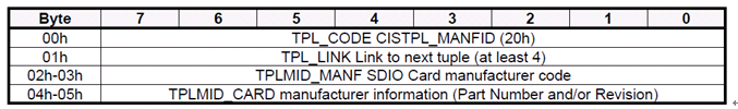
表6 CISTPL_MANFID: Manufacturer Identification Tuple
如上表,sdio设备的id就存储在tuple code(0x20)的tuple中,就是后续扫描中说到的vendor id与device id。
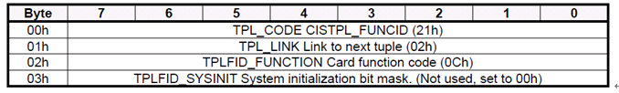
表7 CISTPL_FU
 最低0.47元/天 解锁文章


 10万+
10万+

 被折叠的 条评论
为什么被折叠?
被折叠的 条评论
为什么被折叠?
 到【灌水乐园】发言


