


Chapter 5 Gate Drivers and Level Shifters
5.1 Introduction
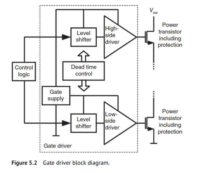
Gate driver如下图所示, 包括功率管(带保护), Gate driver, Level shifter, Gate Supply 和Dead-time control.
5.2 Gate Driver Configurations
Fig 5.3展示了常见gate driver结构. 最常见的为(a)上P下N, 和(d)上N下N. 上P下N常用于Vbat在5V以内. 双N结构用于DC-DC Vbat为高压, 达到100V, 而且NMOS的Ron比PMOS小.
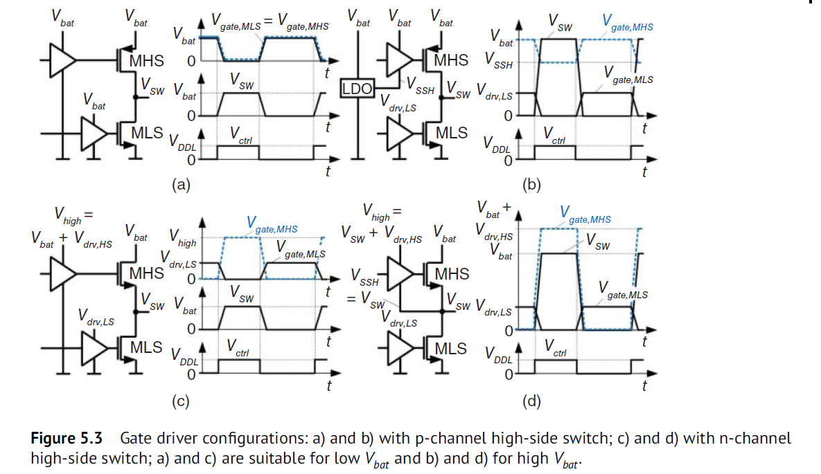
Fig 5.4展示了low-side gate driver
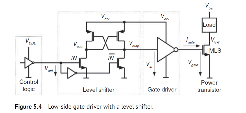
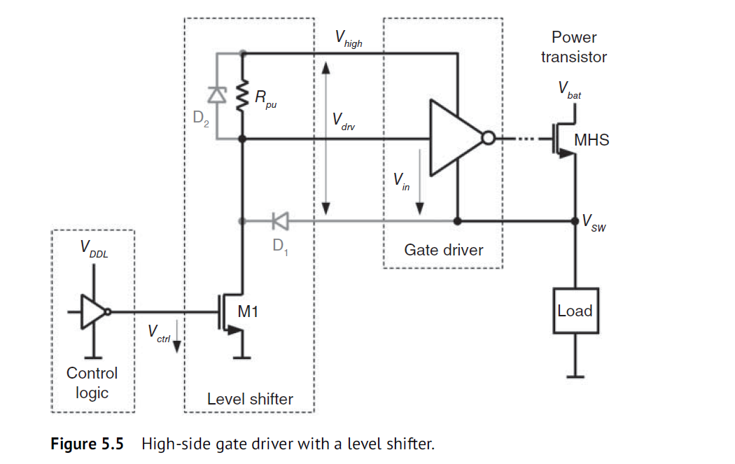
Fig 5.5展示了high-side gate driver. Rpu作为上拉电阻, 确保当Vctrl=0时, Vdrv=Vhigh
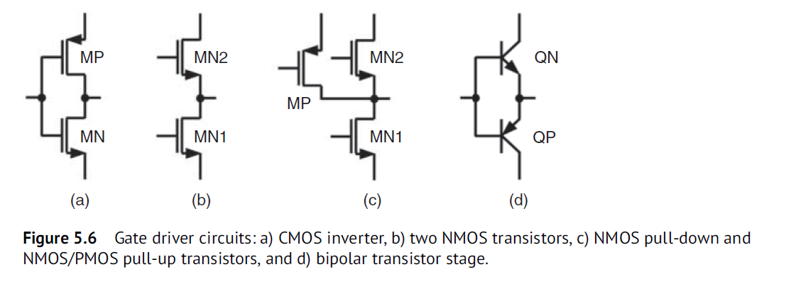
5.3 Driver Circuits
驱动driver电路如Fig 5.6所示.
(a) CMOS结构为最常见结构. (b)为双NMOS结构, 用于没有PMOS场景, 需要bootstrap电路或者charge pump给MN2供电. © 无需bootstrap, MN2接到Vdrv, 在switching开始时导通大量电流, 随着Vsw接近Vdrv, MN2关闭, MP把Vsw最终拉到Vdrv. 因为有MN2, ©中MP的size不用特别大, 不像(a). (d)采用BJT作为driver, 用于驱动高压, 外置power管.
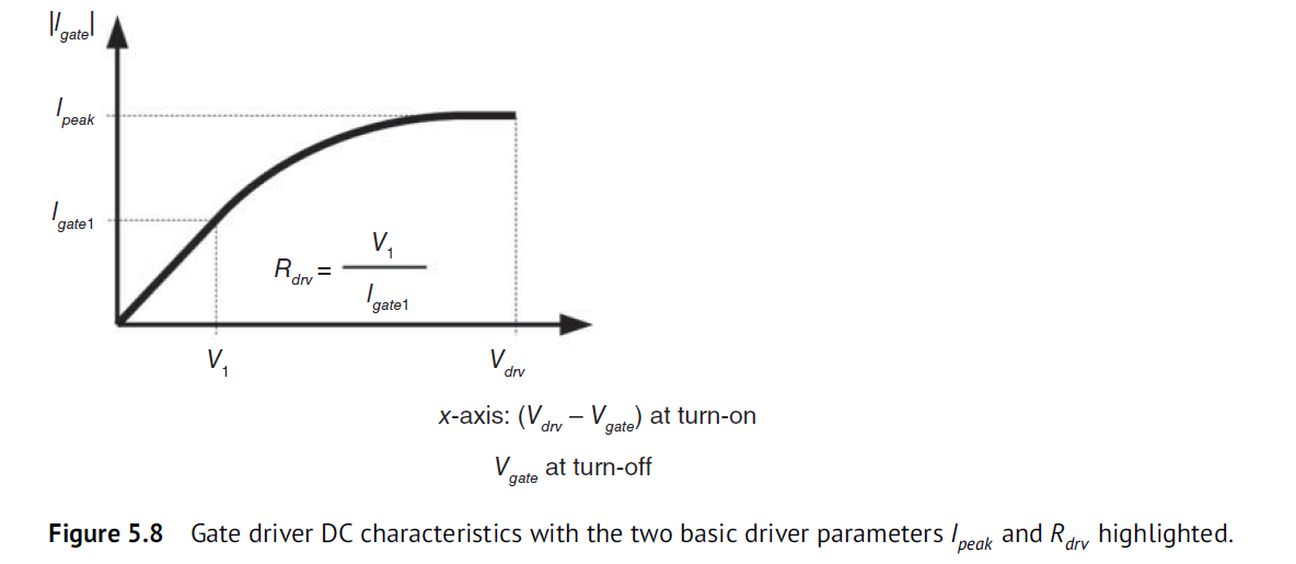
5.4 DC Characteristics
Driver输出的电阻, Rdrv=V1/Igate1, 为1–10 Ω, 峰值电流Ipeak为1-5A, 能估算gate开启时间.
例如Cgate = 200 pF, Vdrv = 5 V, Ipeak = 1A. 开启时间t = Qgate/Ipeak = CgateVdrv/Ipeak = 200 pF ⋅ 5 V / 1A = 1 ns.
Ipeak降为10mA, 则t=100ns.
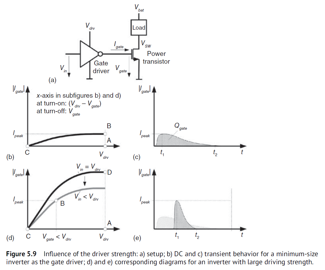
5.5 Driving Strength
driver驱动能力越强, Igate越大, Vgate上升时间越短. 如下图所示
5.6 The CMOS Inverter as a Gate Driver
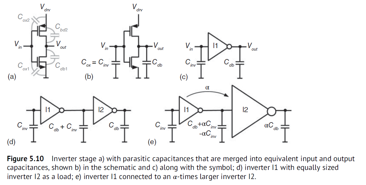
5.6.1 Input and Output Capacitance
inverter的输入和输出电容根据尺寸同比例增加. 后级比前级尺寸增大 𝛼 倍, 电流能力增加 𝛼 倍, 电容增加 𝛼 倍.
5.6.3 Rise-Fall Time
rise, fall time和电流与Charge相关

5.6.4 Average Propagation Delay
delay和charge与电流相关

5.6.5 Power Dissipation
Short Circuit Losses
在input transition阶段, 上下管同时导通, 产生short电流, 能量损失为

Dynamic Losses
dynamic loss为charge和discharge输入电容Cload产生的loss

5.7 Gate Driver with a Single-Stage Inverter
5.7.1 Speed
total propagation delay 总delay=输入delay+输出delay

tin随着放大倍 𝛼 增加, tout随着放大倍 𝛼 减小

可得最优化的比例系数 𝛼 为

5.7.2 Loss Energy
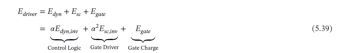
Dirver loss由control logic, gate driver 和 gate charge loss组成

可得最优化的比例系数 𝛼 为

5.8 Cascaded Gate Drivers
可以通过多级级联方式减少propagation delay, 每级尺寸放大倍数为 𝛼
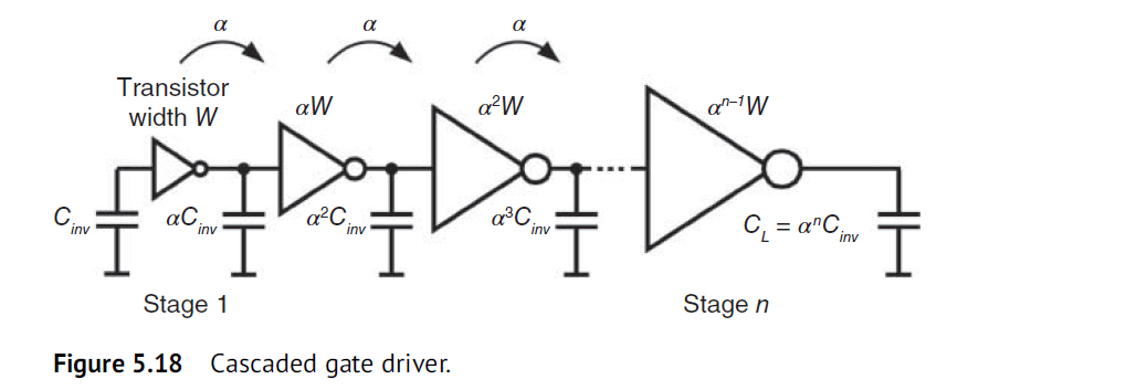
n级总体delay为

5.8.1 Optimization for Speed
可推导出, 为了minimize propagation delay, 𝛼 = e ∼ 2.72
串联级数n为

一般来说级数n不会超过6, n大了功耗太大, delay减小收益有限.
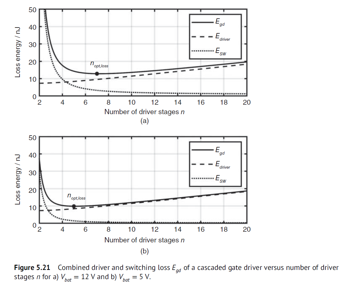
5.8.2 Optimization for Energy Efficiency
考虑节省loss, 整体loss为driver+switching loss, 和供电电压, 多个参数有关

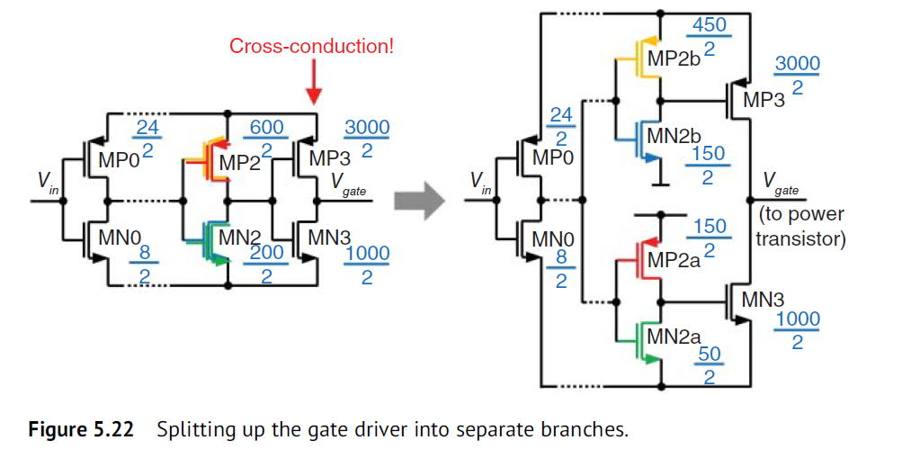
Short-Circuit Losses in the Last Driver Stage
Split-Path Gate Driver
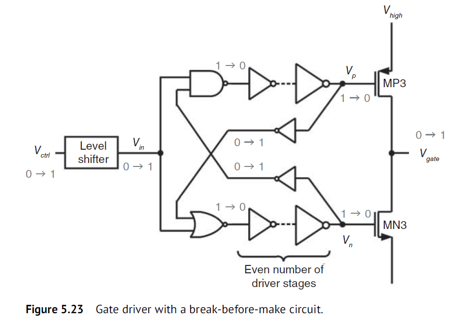
driver最后一级PMOS和NMOS尺寸大, 驱动gate会有较长时间串通, 可用split-path结构, 如下图所示. PMOS和NMOS的size是3:1, 因此split path (MP2b, MP2a)管子的比例也是3:1.
Break-Before-Make Circuit
Break-Before-Make意思是先关后开, 即确保上管关闭后, 再开启下管. 反之确保下管关闭后再开启上管. deadtime会边长, 而且需要高压转低压level-shift.
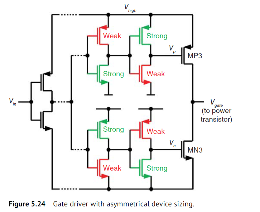
Asymmetrical Sizing
非对称size无需gate反馈信号, 通过driver尺寸, 让MN3关闭速度快, 开启速度慢. MP3也是关闭速度快, 开启速度慢, 避免MP3和MN3串通. 一般asymmetry factor(AF)取20% ~ 30%.
5.9 External Gate Resistor
为了降低开启gate速度, 缓解EMI, 可以添加gate电阻 Rg.
D为damping factor, D = 2∕Q. D一般取0.7, 确保overshoot较小.

5.10 dv/dt Triggered Turn-On
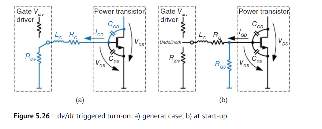
当SW快速翻高或者翻低时, 通过Cgd会给gate注入或者拉出电流, 造成Vgs增加, 功率管误开启, 如下图所示. Igd=Cgd*dVds/dt
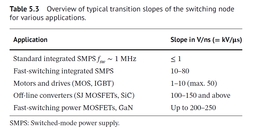
dVds/dt 变化速度, 可达到10V/ns
5.10.1 Integrated Power Stages
对于集成功率级, 忽略inductance, 下拉电阻driver resistance Rdrv+Rg需要小于

5.10.2 Discret e Power Stages
对于分离器件, 考虑环路电感, Cloop ∼ CGS
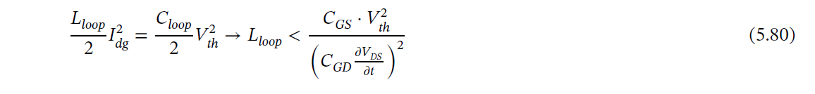
5.10.3 Save Start-Up
启动时由于电源轨没有ready, 容易发生 dv/dt触发开启. 如Fig 5.26(b)所示, 在gate上添加下拉电阻Rg. Rg小了会增加功耗和驱动负载, 可考虑Rg=100k-1M ohm.
5.11 Bootstrap Gate Supply
对于高边的NMOS驱动, 需要提供Vbat(高压)+Vdrv(5V)的高压电源轨. bootstrap提供了一种简单的供电方式, 但需要Vsw周期性为零才能刷新电容Cboot.
5.11.1 General Operation
Bootstrap如下图所示, 当下管开启Vsw为0V时, VDD给Vboot充电达到Vdd-VF. 提供上管开启电压, 当上管开启, Vboot=Vbat+Vdd-VF. Cboot为High Side driver供电, 需要Vsw周期性为零才能补电.
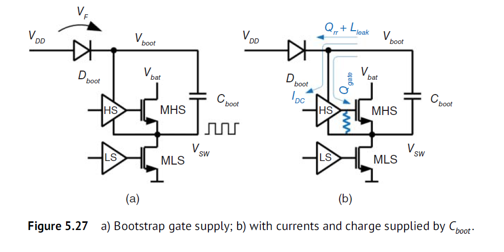
5.11.2 Charge Balance and Bootstrap Capacitor Sizing
Cboot电容需要提供:
- gate charge Qgate来开启上管
- Dboot的 reverse recovery charge Qr
- Dboot的leakage电流
- gate driver和level shifter的静态电流
- gate-source的leakage电流 (包括下拉电阻产生的)
静态leakage电流记为Iboot, 在上管开启时存在, 开启时间记为Dmax/fsw, 因此

ΔVboot 取 10% of Vdrv 即0.5V, Cboot最小电容值有要求:

gate charge Qgate占最主要因素

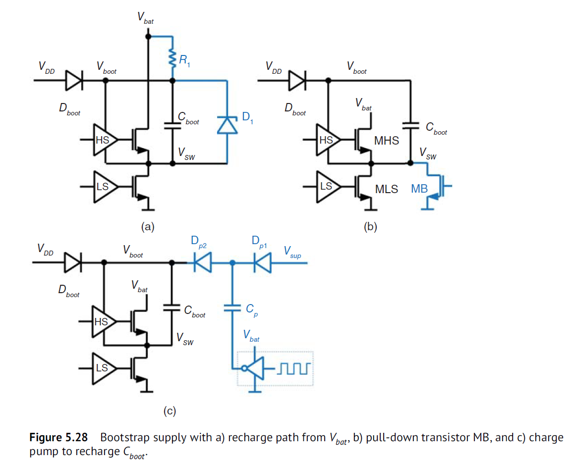
5.11.3 Practical Aspects of Bootstrapping
一些bootstrap结构如下图所示.
Fig.5.28(a) 采用R1给Cboot充电, Zener D1钳位Vboot电压, R1取值100 kΩ
Fig.5.28(b) 采用MB把Vsw下拉到 gnd, 作为 power-on-reset
Fig.5.28© 采用charge pump提供Vboot, 无需Vsw为0V.
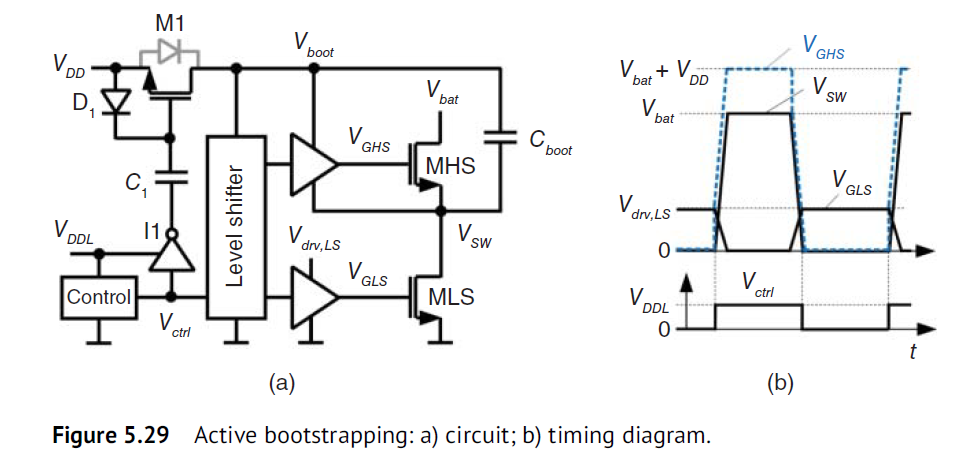
5.11.4 Active Bootstrapping
为了增加上管开启电压, 避免VF drop, 可用active bootstarp, 即用NMOS管替代diode, 如下图所示. D1, C1和I1形成了local bootstrapping to turn on the
transistor M1. M1的方向很重要, 体二极管一定要block Vboot和VDD.
5.12 Level Shifters
level shifter转换高低电平, 是核心器件.
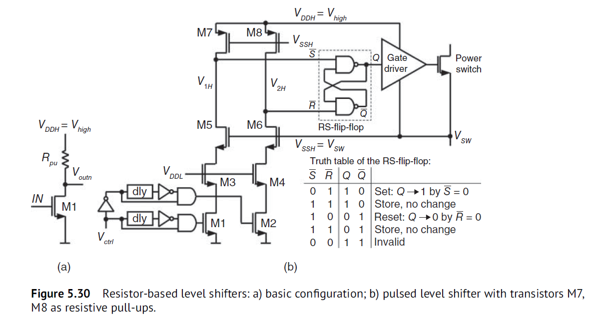
5.12.1 Resistor-Based Level Shifters
Fig. 5.30a)为最简单的电阻LS, IN=0时靠Rpu把Voutn上拉到Vhigh, IN=1时, Voutn=Vhigh-I1*Rpu. 需要用diode来钳位, 如同Fig5.5. 另外还有功耗损失, 对Bootstrap的供电有要求. Rpu一般取值100kΩ.
Pulsed Level Shifter
为了减少loss, 可参考Fig 5.30(b), M7和M8取代了Rpu, M1和M2产生短pulse, gate电压由nand组成的RS-flip-flop控制. 开启M1,M2, 下拉V1H, V2H, 造成RS latch输出翻转. M3和M4为高压器件, 用来保护M1和M2. M5和M6形成common-gate gain结构, 用来放大M3和M4的drain电压, 因此加速level-shifter. 同时M5和M6的体二极管能确保V1H和V2H不会低于Vsw-VF, 保护了M7和M8, 和RS latch.
M1和M2输入为短pulse, either V1H or V2H experience a negative pulse and set the RS flip-flop accordingly. 在稳态时, M1和M2 off, V1H和V2H 为高, 因此RS latch输出保持.
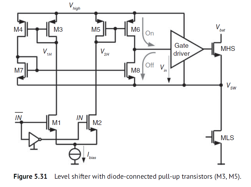
Level Shifter with Diode-Connected Pull-Up Transistors
Rpu可以换成diode-connected transistor, 如下图Fig 5.31所示. 此结构提供 differential signal transfer, 抗coupling和寄生效应能力更强. M1和M2的输入反向, M3到M8形成symmetrical amplifier. IN=1时, M2流过Ibias, M5和M6 把gate driver Vin上拉到Vhigh. IN=0时, Vin被下拉到Vsw. Ibias可设计成adaptive, 在signal transfer时值最大, 在steady state时值变小来减少功耗. 可用简单的inverter+delay chain实现, 翻转时Ibias为mA, 静态时为5uA.
该结构可工作在10MHz, 可通过precharge M3和M5的Vgs来加速翻转. 可通过在M3和M5的drain添加下拉电阻. 同时M3和M5的尺寸要取小. 该结构的缺点是, M3和M5 fast slope时, Vsg下降厉害, 可能会超过maximum Vsg rating. 因此可加D1和D2来保护V1H和V2H. 为了加速翻转, 可以比较V1H和V2H电压压差, 100mV就行了.
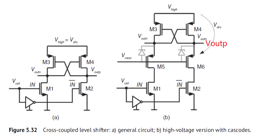
5.12.2 Cross-Coupled Level Shifters
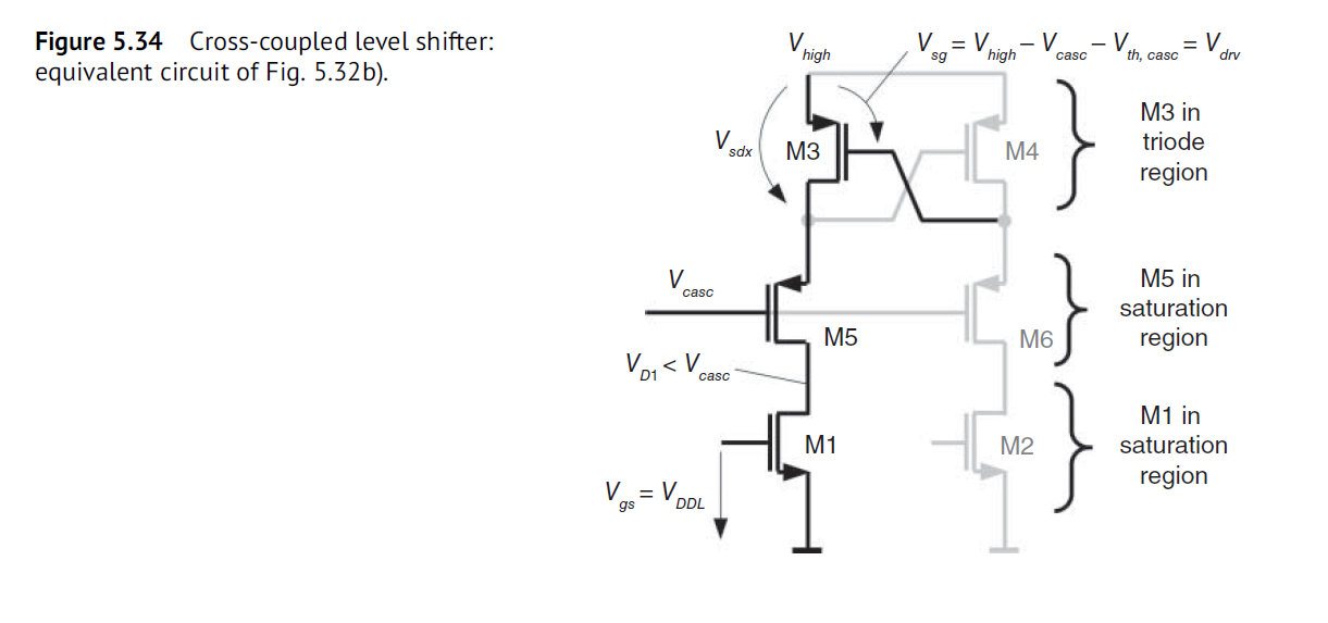
Cross-coupled level shifter如下图所示, 类似latch. 低压(a)需要确保Vhigh<5V. (b)展示了高压level shifter, M3和M4的Vsg被casecode管保护.
Due to the two phases, the cross-coupled level shifter is relatively slow. One output signal switches faster than the other one. cross couple latch 翻转速度较慢, 一边速度比另外一边快, 而且没有静态电流功耗.
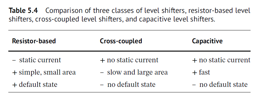
resistor-based, cross-coupled level shifter和 coactive level shifter对比如下
Default State
由于对称性, cross-coupled没有初始态, 在电源轨启动时可能有问题. 可以添加几MΩ的上拉电阻定初始态. 或者用power-on-reset (POR) 信号直接下拉Voutp, 直到Vhigh建立好后再释放.
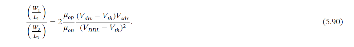
Analysis of the DC Switching Condition, Sizing Equation
M1的下拉能力需要比M3的上拉能力强, latch才能翻转. M1工作在饱和区, M3工作在线性区, M1的W/L size要远大于M3. W1和W3尺寸关系
Sizing of the Cascoded Cross-Coupled Level Shifter
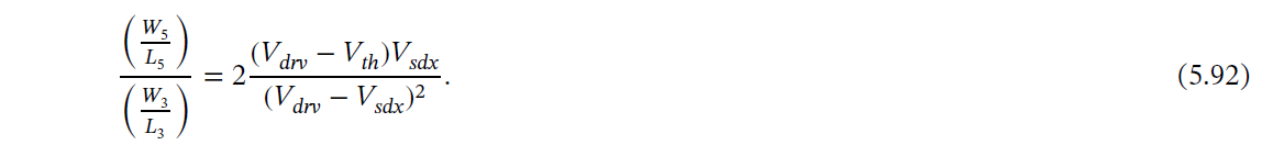
LS的输出为Vcasc + Vth,casc ∝ Vcasc, 当M3的drain电压下降时, M5的驱动能力也下降, 因此M5和M6的 W/L尺寸要大. M5工作在饱和区
W5和W3尺寸关系
Design Guideline for Cross-Coupled Level Shifters
(1) L 取最小尺寸, 来减小寄生电容
(2) W1和W3满足(5.90)和(5.92), 设Vdsx=Vthp,
(3) 增加Vdsx到1.5×Vthp, 计算出W1, W3和W5来加快速度.
Improvements of the Cross-Coupled Level Shifter
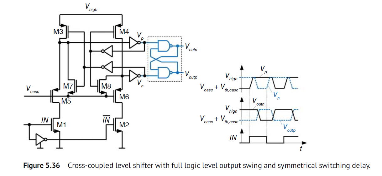
Vcasc电压=Vsw, 因此M3和M4的drain电压最低为Vsw+Vsg5, M3和M4被保护了, 但是输出电压最低为Vsw+Vsg5, logic “0” 可能不正确. 为了解决这个问题, 可以加入M7和M8, 如Fig5.35(a), 将输出电压彻底拉到Vsw即’0’. Fig 5.35(b)加入inverter, 增加loop gain, M7和M8可取最小尺寸, 能加速且功耗更小.
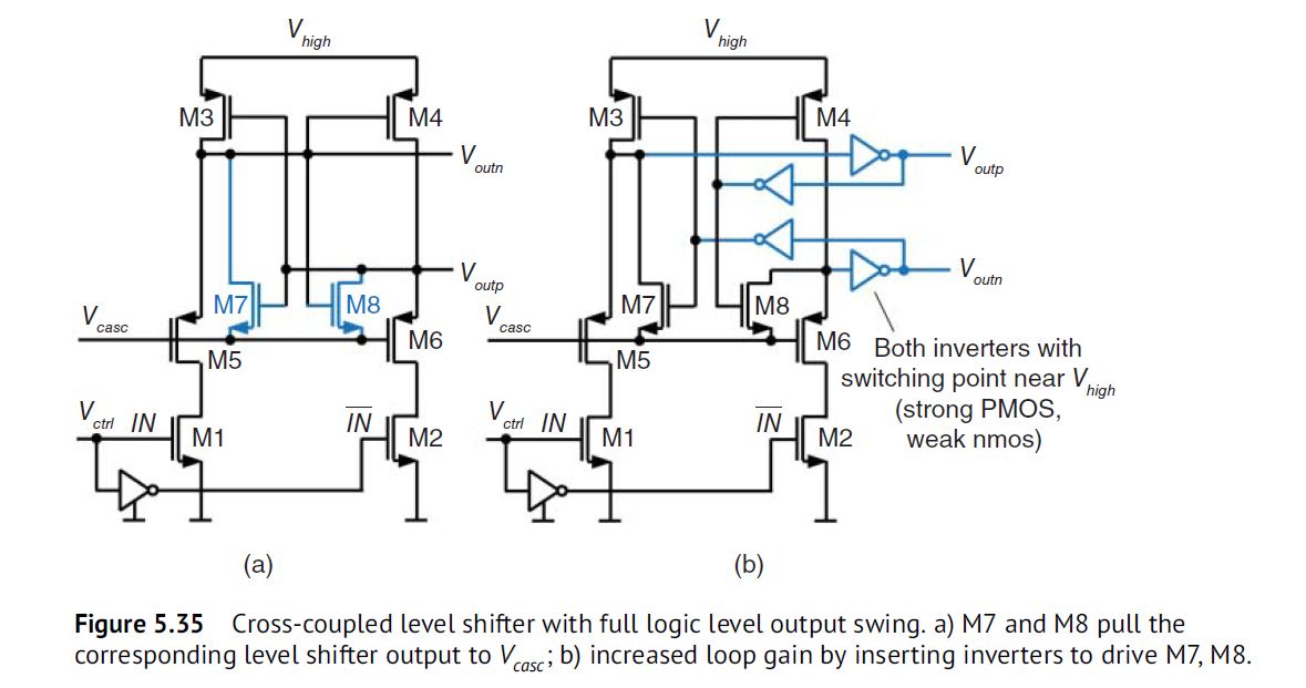
Figure 5.36是Fig5.35(b)的拓展, 通过RS latch解决了asymmetrical switching delays. 输出仅在最慢transition阶段变化, VP或VN的下降沿才会改变Voutn和Voutp. 因此输出更加对称.
5.12.3 Capacitive Level Shifters
capacitive level shifter 如下图Fig. 5.37所示. Cc transfer V1L和V2L到V1H和V2H, I5整形输出波形. 电容Cc需要抗住VDDH的电压. Cc可到50 fF级别.
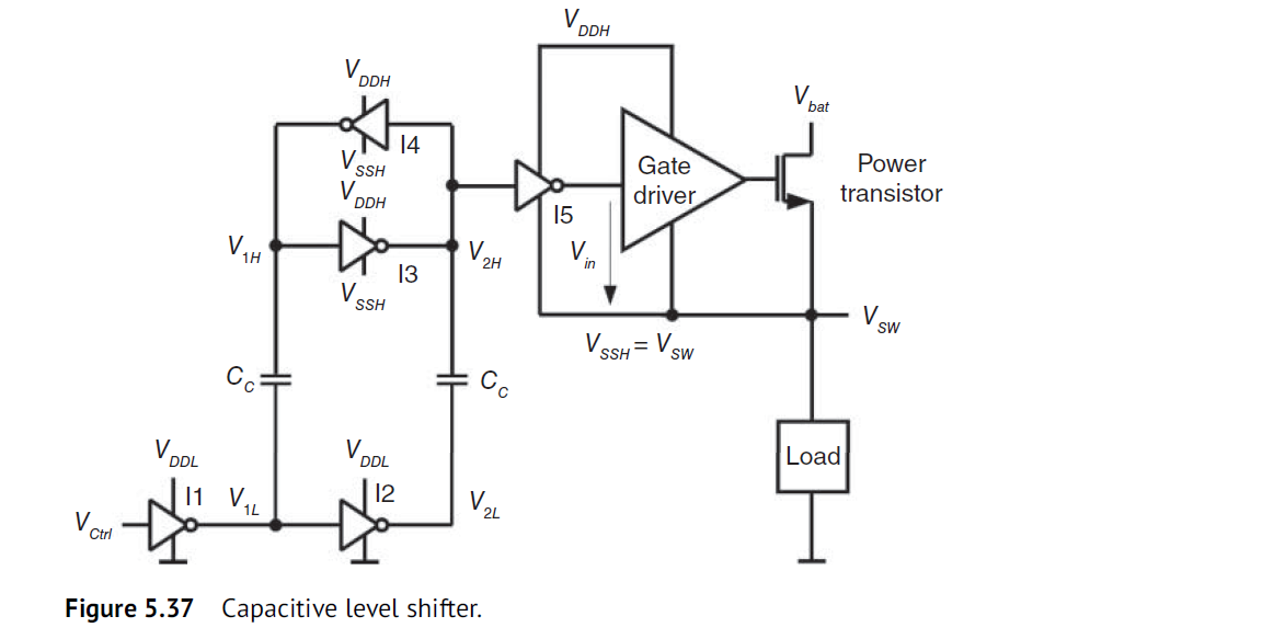
Open-Loop Model
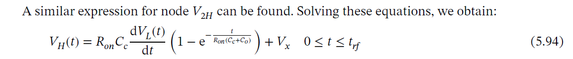
VH表达式
Design Guideline
(1) 定I3和I4的尺寸: Ron需要足够大, V1H和V2H才能follow V1L和V2L, Ron ≈ 10 kΩ
(2) Sizing of Cc: Cc需要比I1和I2的寄生电容大, 增加Cc来减小delay
(3) 定I1和I2尺寸: 需要strong inverter
(4) Fine-tune the level shifter
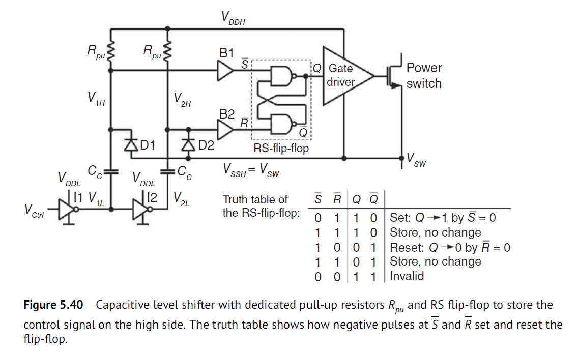
Capacitive Level Shifter with Pull-Up Resistors and RS Flip-Flop
不用cross-coupled inverters, 采用tens of kΩ的Rpu, 再配合低电平有效的RS latch 如下图所示. D1和D2钳位保护V1H, V2H不低于Vsw.
5.12.4 Level-Down Shifters and Ground Level Shifters
level-down的shifter 应用于adaptive dead time, sensing gate信号的场景. Fig 5.41展示了level-down的shifter. 可用a) Resistor-based 或者 b) cross-coupled.
需要注意器件耐压, 确保能低压器件不能看到高压, 可加高压器件或者diode进行clamp.
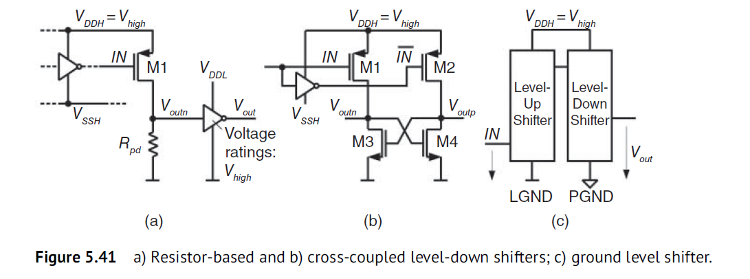
c) 展示了 从logic ground (LGND) 到 power ground (PGND) 转化, 确保寄生bond wire产生的毛刺不会引起信号传输错误, 提高signal integrity. level-shifter可用(b)中的结构.
5.13 Common-Mode Transient Immunity
switching node的上升/下降速度 可能达到100V/ns, 带来coupling, 如下图所示
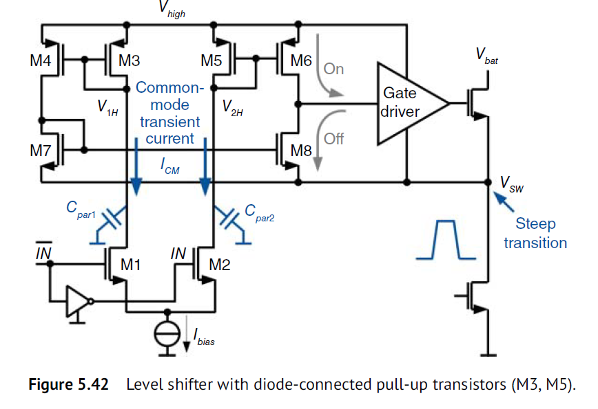
V1H和V2H到地的寄生电容Cpar = 10 pF , dVsw/dt = 10 V/ns, transient共模电流Icm达到100mA. 而Ibias也才10uA, 共模电流Icm可能造成shifter输出状态错误.

考虑1% mismatch,Cpar1=10pF, Cpar2=9.9pF, ΔICM = 1 mA, 也会淹没Ibias=10uA.
Common-mode transient immunity (CMTI) 共模瞬态免疫性就重要了, 采用Fig 5.40的RS latch结构的CMTI就很好. 当Vsw迅速上升时, Rpu给Cpar充电, V1H和V2H有negative pulse. D1和D2确保V1H和V2H不低于Vsw-diode, 保护B1和B2不会超压. 这是invalid state, 需要加入blanking电路来屏蔽. 当Vsw迅速下降时, Cpar放电, V1H和V2H有positive pulse. V1H=V2H=Vhigh, store, RS latch输出保持. 注意V1H和V2H可能超过Vhigh, 需要加入clamp电路.
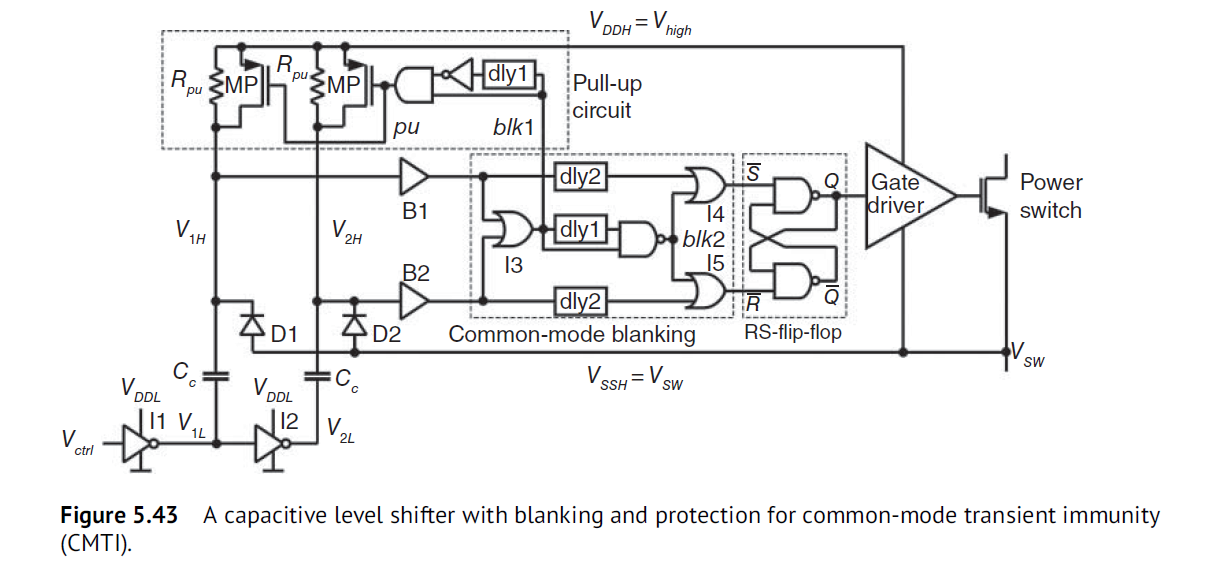
改进的电路如Fig 5.43所示, 加入了共模检测和blanking电路. 当Vsw快速上升时, B1和B2检测的0, 输出给OR门I3,I3 detects the transient and generates two blanking signals, blk1 = 0 and subsequently a positive pulse blk2 (delay stage dly1, 8 ns in [22]). A delay stage dly2 (3 ns in [22]) is inserted in the signal detection path such that the blanking is always detected before the signal propagates to the RS flip-flop. While blk2 = 1 the connected NOR gates I4, I5 each provide 1-level such that S = R = 1 and the flip-flop safely keeps its state. After detecting the rising transition, the output signal blk1 of NOR gate I3 generates a pulse pu, which activates both transistors MP and pulls V1H and V2H up to Vhigh. This way, the level shifter reaches its default state quickly and can receive the next signal at maximum speed. Both MP devices turn off at the end of the pulse pu, and the pull-up is only formed by Rpu. As outlined in Section 5.12.3 for the level shifter in Fig. 5.40, a fast reaction can be achieved for larger values of Rpu (>10 kΩ).
RS latch也可用NOR组成, 上拉电阻换成下拉电阻到Vsw. 这样default和reset state就是0. Positive pulses set and reset RS latch.
[22] Rindfleisch, C., Otten, J., and Wicht, B. (2022) A highly-integrated 20-300V 0.5W active-clamp flyback DCDC converter with 76.7% peak efficiency, in 2022 IEEE Custom Integrated Circuits Conference (CICC), pp. 1–2, doi: 10.1109/CICC53496.2022.9772834.


 被折叠的 条评论
为什么被折叠?
被折叠的 条评论
为什么被折叠?
 到【灌水乐园】发言


