


Chapter 24 Operational Amplifiers I
operational amplifier (op-amp) 运算放大器无疑是模拟电路中最基础最重要的block之一.
这一章我们将review op-amp一些重要参数包括:AOL (open-loop gain), CMR (common-mode range on the input), CMRR (common-mode rejection ratio), PSRR (power supply rejection ratio), output voltage range, current sourcing/sinking capability, and power dissipation.
The Two-Stage Op-Amp
基本的 two stage op-amp:
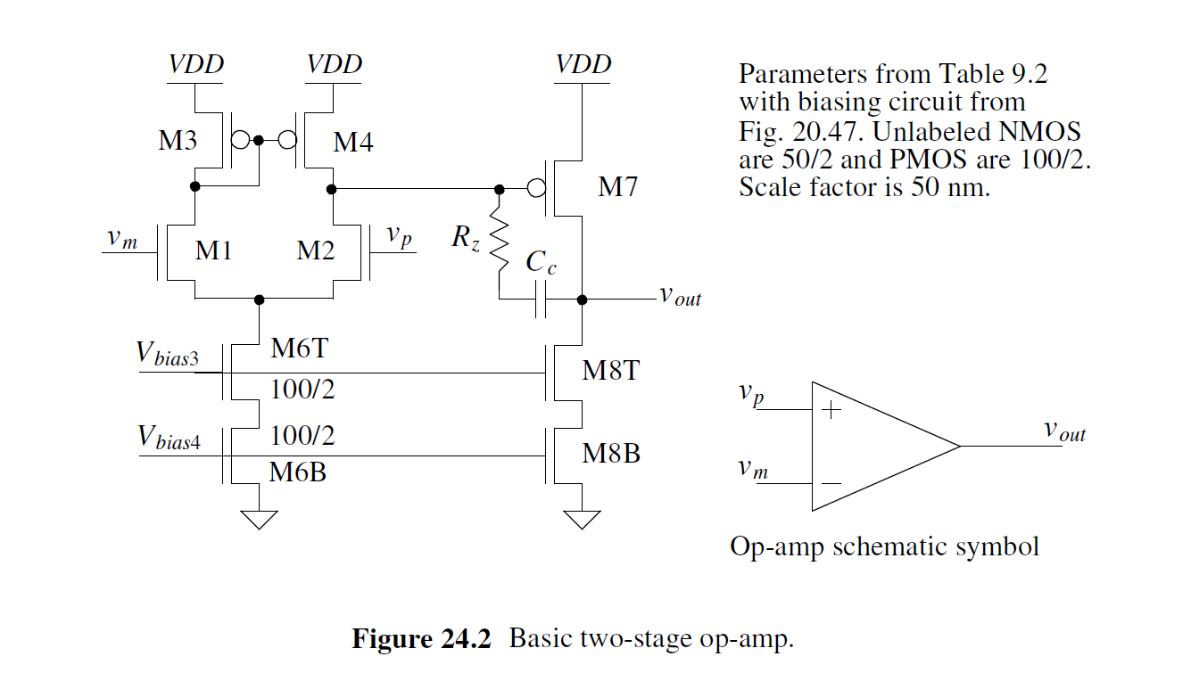
低频开环增益Gain:
Input Common-Mode Range 前面已谈
Power Dissipation 前面已谈
Output Swing and Current Sourcing/Sinking Capability
Because this topology can source a considerable amount of current, it is useful as a voltage regulator (because the op-amp is always only sourcing current in a voltage regulator application). 这种结构可以提供(source)电流, 因此可作为稳压器.
Offsets
一种是random offset, 主要靠加大device尺寸等手段减小
一种是systematic offset. 例如M7和M8 design 的电流不一致, 导致output发生偏移. 可能是故意所为. A systematic offset is the result of poor sizing choices or it can be an artifact of sizing a device to attain a specific design goal (such as making M7 wider so it can source more current).
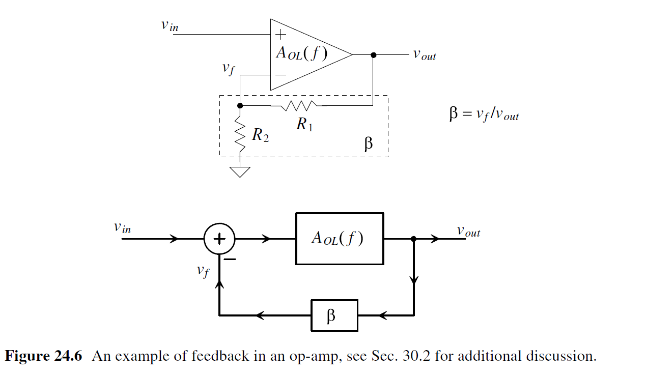
Compensating the Op-Amp
A
C
L
(
f
)
=
V
O
U
T
V
I
N
=
A
O
L
(
f
)
1
+
β
⋅
A
O
L
(
f
)
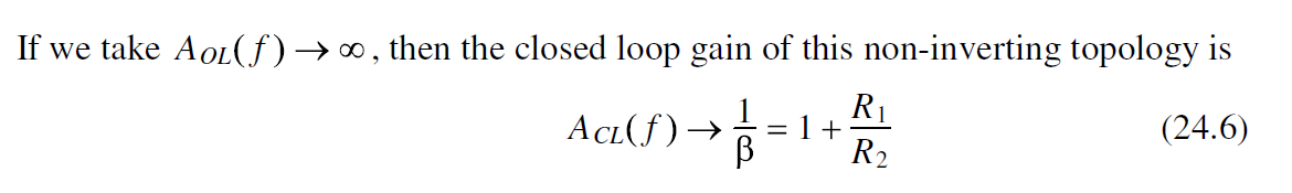
A_{CL}(f)=\frac{V_{OUT}}{V_{IN}}=\frac{A_{OL}(f)}{1+\beta\cdot A_{OL}(f)}
ACL(f)=VINVOUT=1+β⋅AOL(f)AOL(f)
判断op-amp环路稳定性: To determine the stability of an op-amp, we’ll look at the open loop gain when the feedback factor is one, that is,
∣
A
O
L
(
f
)
=
1
and
∠
A
O
L
(
f
)
=
18
0
∘
∣
\left| A_{OL}(f)=1 \text{ and } \angle A_{OL}(f)=180^{\circ } \right|
∣AOL(f)=1 and ∠AOL(f)=180∘∣
看开环增益AOL=1处的phase margin或者AOL phase=180时的gain margin.
一般来说, beta越小(the less output signal we feed back), 环路越容易稳定,Voltage follower or unity feedback最难稳定.
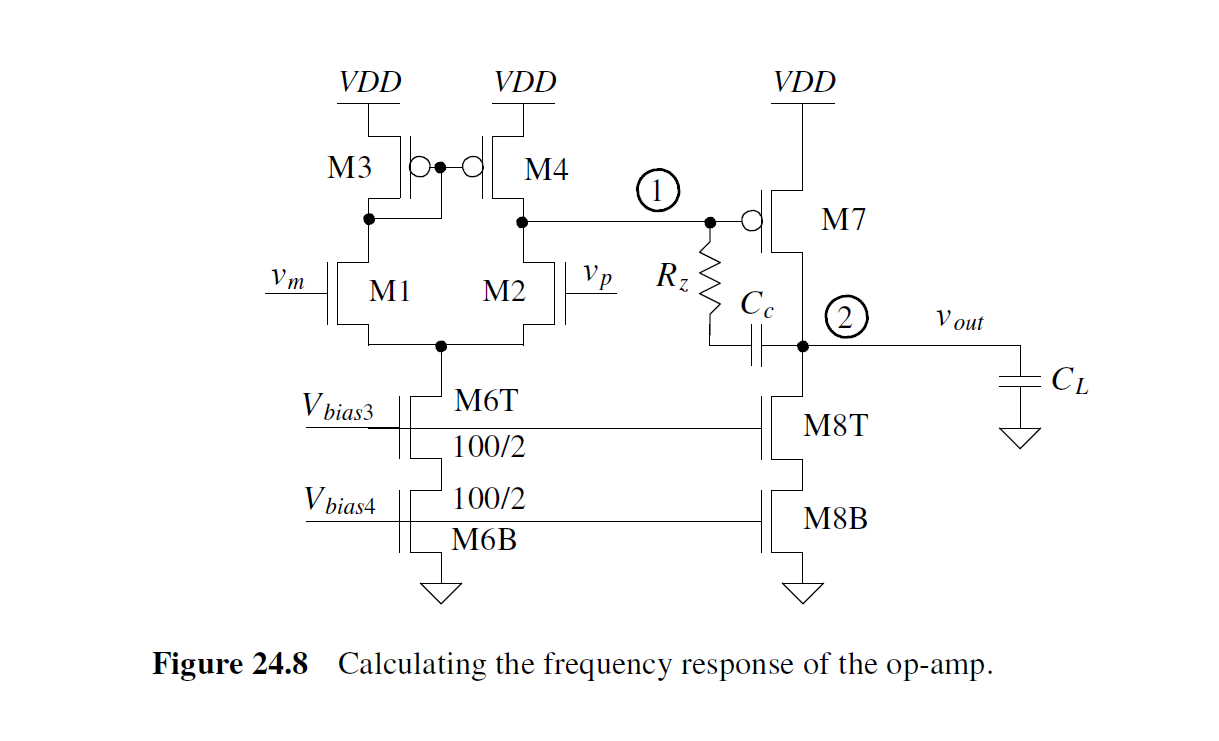
dominant pole: at net 1, 带Miller Cap fst = 1/(gm2 * R1 * R2 * CC) = 290K
Second Pole: 由于pole splitting: fnd = gm2*Cc/(Cc C1 + C1C2 + CcC2) = 210MHz
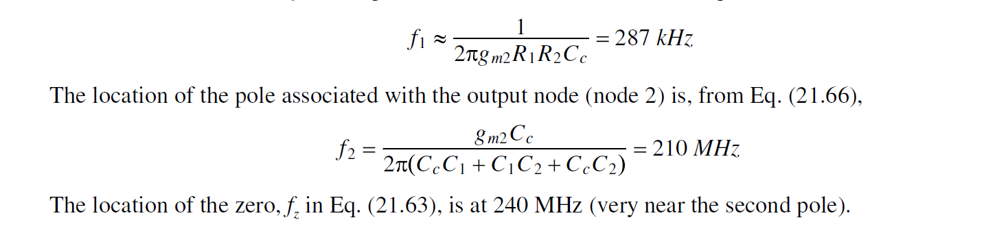
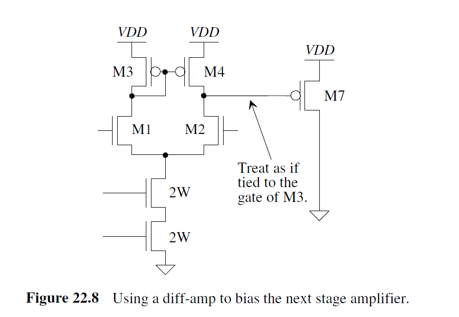
Zero: fz=gm2 / (Cc) = 240MHz, 接近second pole, 这里gm2=gm7 (Fig 24.8)
Gain and Phase Margins
We want the open loop gain of the op-amp to be much less than one when the phase shift is 180°.
To determine an op-amp’s Phase Margin, we look at the phase shift when the open-loop gain is unity. The amount of phase shift away from 180° is the PM of the op-amp. 180° - phase shift = PM
To calculate the Gain Margin, we look at the difference between the open-loop gain and unity when the phase of the op-amp is 180°
Removing the Zero
RHP右零点=gm2/Cc, 为了消除RHP可以加入nulling resistor Rz=1/gm2, 或者 Rz>1/gm2把右零点推到左零点, 这里gm2=gm7 (Fig 24.8).
The practical problem with using Rz is that setting its value to a precise number (say 1/gm2) is challenging with shifts in process, temperature, or voltage. 由于工艺或者电压偏差, Rz的值会变化.
一个解决方法: 采用工作在triode region的MOSFET代替resistor, 如下图所示
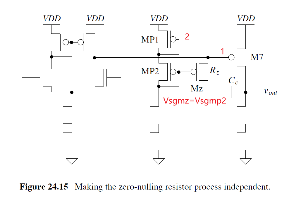
Ideally, the source-gate voltage of M7 is the same as the VSG of MP1. It then follows that the source-gate potential of MP2 equals the source-gate potential of Mz. The channel resistance of Mz is then,set to 1/gm2.
Set VsgM7=VsgMP1, then VsgMP2=VsgMz, then Mz的工作在线性区 resistance可定.
The practical issues with this method are the wasted power dissipated by the additional circuitry and the fact that if the output swing becomes large (especially at higher frequencies where Cc has a small impedance), Mz can move out of the triode region, which can affect the large-signal behavior of the op-amp. 潜在问题是additional power dissipation, 另外在wide output swing下, Mz可能不工作在线性区, 可能影响op-amp大信号表现.
还有一种办法是在Cc回路上串联 +1 gain buffer. 如下图所示
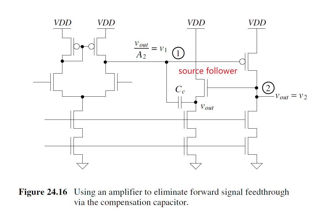
A source follower allows the output signal to feed back through the compensation capacitor (so that the pole-splitting effect is still present). However, the root cause of the RHP zero, namely, Cc shorting the input of the second stage (the output of the diff-amp) to the output of the second stage (the output of the op-amp) at higher frequencies is removed.
设计思路: 保留feedback through Cc, 斩断 short 2nd input with 2nd output这条路
The concerns with this topology are, again, power dissipation and, perhaps more importantly, large signals. If the overall output voltage swings too low, it causes the source-follower to shut off.
问题仍然是power和source follower might shut off at large Vout swing.
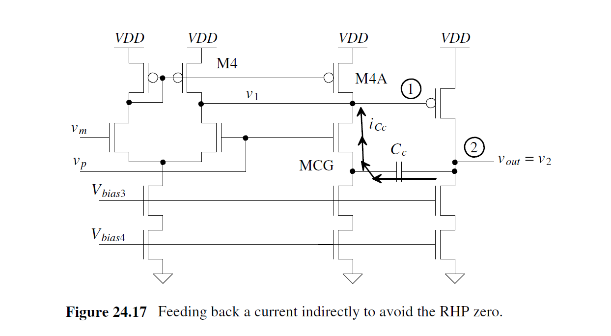
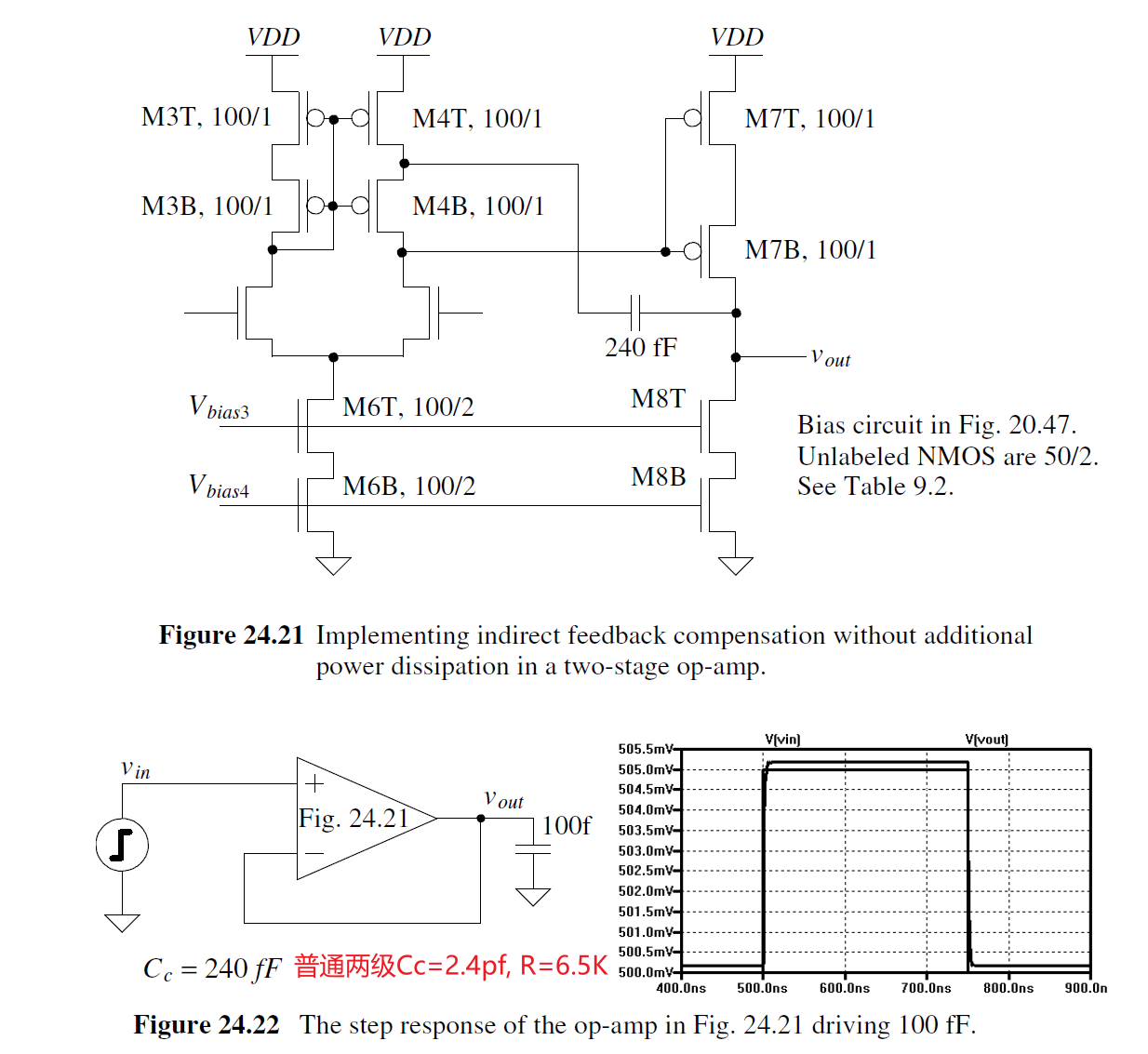
Compensation for High-Speed Operation - Indirect feedback
i
C
c
≈
v
o
u
t
1
/
j
ω
C
c
i_{Cc}\approx \frac{v_{out}}{1/j\omega Cc}
iCc≈1/jωCcvout
The added MOSFETs form a common-gate amplifier. (Note that here we are assuming vp << vout , so the source-follower action of MCG is negligible. MCG is connected to vp to set its gate at the DC voltage of the input.) The current iCc is fed back through the common-gate MOSFET (MCG), to node 1 (the output of the diff-amp).
假设vp <<vout, icc从MCG(common gate) 送到了 note1
小信号模型:
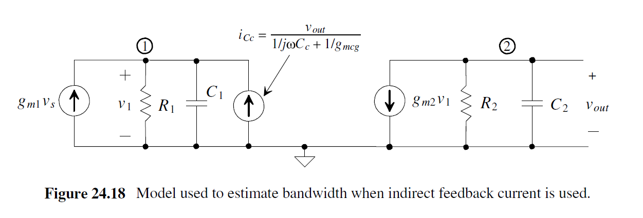
传输函数:
产生了左零点 LHP, 有益于 compensation. fz=gmcg/(Cc)
At high speeds the phase shift through Cc will cause the output signal to feed back and add to the signal at node 1. This positive feedback enhances the speed of the op-amp.
first pole:
f
1
=
1
2
π
g
m
2
R
2
R
1
C
c
f_{1}=\frac{1}{2\pi g_{m2}R_{2}R_{1}C_{c}}
f1=2πgm2R2R1Cc1
second pole:
f
2
=
g
m
2
C
c
2
π
C
1
(
C
L
+
C
c
)
f_{2}=\frac{g_{m2}C_{c}}{2\pi C_{1}(C_{L}+C_{c})}
f2=2πC1(CL+Cc)gm2Cc
The location of the second pole is at a considerably higher frequency using this technique.(second pole更远) The result is that we can set the unity gain frequency to a higher value and still have a stable op-amp (GBW更高也能保持稳定性). Further, the load capacitance (which is included in C2 ) can be considerably larger for a given PM or GM.
GBW (unity-gain frequency, fun)
f
u
n
=
g
m
1
2
π
C
c
(
≈
f
z
if
g
m
1
≈
g
m
c
g
)
f_{un}=\frac{g_{m1}}{2\pi C_{c}}(\approx f_{z} \text{ if } g_{m1}\approx g_{mcg})
fun=2πCcgm1(≈fz if gm1≈gmcg)
采用 Indirect feedback 电路最大的好处就是可以大幅减小Cc的容值, 也就是面积, 但会额外增加power dissipation.
可以采用下图, 也是Indirect feedback. The current through the compensation capacitor is fed back through M4B to the output of the diff-amp. (这种结构很实用!)
注意: indirect feedback的接法很灵活, 关键是确保Cc反馈点和第二级的gate同一方向变化.
Slew-Rate Limitations
Fig. 24.8 Vp从0.5V->0.9V-0.5V的step-response 如下图所示
关键在于Id_M8去充电或者放电Cc电容. 在Vp下降时, node1上升, 会通过Cc couple 输出上升, which is so bad!

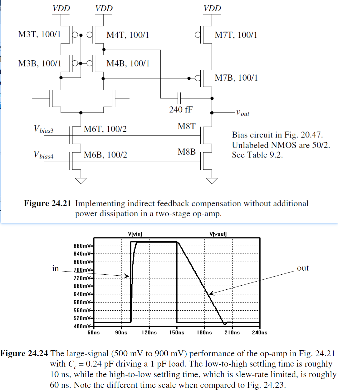
采用Fig 24.21的结构再做step response:
由于Cc变成1/10, slew-rate要好得多.
Because of the improved speed performance, smaller layout area, and (as we’ll see) better power supply noise rejection, we’ll use indirect compensation in place of Miller compensation in the remaining two-stage op-amps that we discuss in this book. Indirect compensation is the result of connecting the compensation capacitor back to a low-impedance node rather than a high impedance node was done in Fig. 24.8. In practical op-amp designs one should never connect a compensation capacitor back to a high-impedance node.
Indirect feedback将Cc接到low-impedance node, 而不是像传统的miller补偿两级运放接到high-impedance node. Indirect feedback的速度更快, 面积更小, PSRR更好, 因此对于miller补偿电路, 我们都会采用Indirect feedback. 在实际中我们永远避免把补偿电容接到高阻节点!
Common-Mode Rejection Ratio (CMRR)
The common-mode gain of the diff-amp is Ac . The common-mode gain of the op-amp is Ac * A2. The differential gain of the op-amp is Aol = Ad * A2
CMRR
=
20
⋅
∣
l
o
g
A
O
L
(
f
)
A
c
⋅
A
2
∣
=
20
⋅
∣
l
o
g
A
d
⋅
A
2
A
c
⋅
A
2
∣
=
20
⋅
∣
l
o
g
A
d
A
c
∣
\text{CMRR}= 20\cdot \left|log\frac{A_{OL}(f)}{A_{c}\cdot A_{2}} \right|= 20\cdot \left|log\frac{A_{d}\cdot A_{2}}{A_{c}\cdot A_{2}} \right|=20\cdot \left|log\frac{A_{d}}{A_{c}} \right|
CMRR=20⋅
logAc⋅A2AOL(f)
=20⋅
logAc⋅A2Ad⋅A2
=20⋅
logAcAd
CMRR对input offset的影响:
输入共模电压变化/CMRR = 输入offset:
Δ
V
O
S
=
Δ
V
o
A
O
L
=
Δ
V
c
⋅
A
c
m
A
O
L
=
Δ
V
c
C
M
R
R
\Delta V_{OS}=\frac{\Delta V_{o}}{A_{OL}}=\frac{\Delta V_{c}\cdot A_{cm}}{A_{OL}}=\frac{\Delta V_{c}}{CMRR}
ΔVOS=AOLΔVo=AOLΔVc⋅Acm=CMRRΔVc
Delta_Vc=输入common-mode voltage变化.
Power Supply Rejection Ratio (PSRR)
The power supply rejection ratio (PSRR) is a term used to describe how well an amplifier rejects noise or changes on the VDD and or ground power buses.
PSRR用来表示op-amp输出对电源VDD或者地变化/噪声的抗干扰能力
PSRR的Testbench
PSRR VDD的定义:
P
S
R
R
+
=
A
O
L
(
f
)
v
o
u
t
/
v
+
PSRR^{+}=\frac{A_{OL}(f)}{v_{out}/v^{+}}
PSRR+=vout/v+AOL(f)
PSRR VSS的定义:
P
S
R
R
−
=
A
O
L
(
f
)
v
o
u
t
/
v
−
PSRR^{-}=\frac{A_{OL}(f)}{v_{out}/v^{-}}
PSRR−=vout/v−AOL(f)
Ideally, Vout doesn’t vary with changes in VDD and ground (and so the PSRR is infinite).
注意 Fig. 24.27c, where vout/v+ is one. 因此提高差分增益很有必要. Indirect feedback compensation 的GBW更大, 因此高频时PSRR更好.
Increasing the Input Common-Mode Voltage Range
增大输入电压范围, 可以考虑下图rail-to-rail op-amp结构
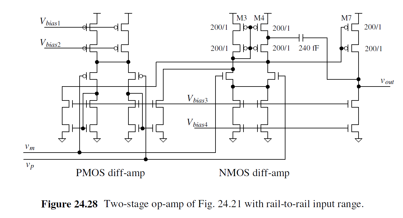
注意输入电压高时nmos 开启, 输入电压低时pmos 开启, gm vary from gmn to gmn + gmp to gmp.
Estimating Bandwidth in Op-Amp Circuits
A
O
L
(
f
)
=
A
O
L
D
C
1
+
j
f
f
3
d
B
A_{OL}(f)=\frac{A_{OLDC}}{1+j\frac{f}{f_{3dB}}}
AOL(f)=1+jf3dBfAOLDC
unity-gain frequency也称为Gain-Band with Product (GBW): at f >> f3B
f
u
n
=
G
B
W
=
A
O
L
D
C
⋅
f
3
d
B
f_{un}=GBW=A_{OLDC}\cdot f_{3dB}
fun=GBW=AOLDC⋅f3dB
对于负反馈环路, 其closed-loop bandwidth (f3dBCL)不会超过开环的bandwith:
A
C
L
⋅
f
3
d
B
C
L
=
f
u
n
=
gain-bandwith product
A_{CL}\cdot f_{3dBCL}=f_{un}=\text{gain-bandwith product}
ACL⋅f3dBCL=fun=gain-bandwith product
例如GBW=100Mhz. 如果负反馈环路gain=10, 其bandwith=10MHz.
An Op-Amp with Output Buffer
上面的op-amp其低频增益都取决输出电阻. 如果输出电阻小, 低频增益也变小.
为了驱动小的输出阻抗, 我们可以加入一个source-follower的buffer, 但是可能会限制输出摆幅 (limit output swing). 另一种方法就是采用push-pull架构作为输出级. 注意push-pull的gain > 1, 如果直接串联之前的op-amp, 我们就有a three-stage op-amp. A three-stage op-amp can be challenging to compensate over production corners (and temperature). 三级运放是很难补偿的.
因此我们可以设计两级运放, 第一级gain较大, 第二级用push-pull, gain较小
第一级采用casecode, 第二级用push-pull如下图所示. 采用indirect compensation current to node 1, we connect the compensation capacitor to the source of M2T, 确保更好的PSRR.
注意: 这种结构也是indirect feedback, 确保Cc反馈点和第二级的gate同一方向变化.
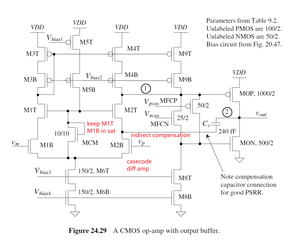
考虑输入step response: Vin 100mV跳变到900mV.
在Chapter 9中我们强调过基本法则: For high-speed design, we must use minimum length devices. 如果我们把所有device的length由2改为1, 那么系统相应会更快, issue就是op-amp gain变差.
The Operational Transconductance Amplifier (OTA)
The operational transconductance amplifier (OTA) can be defined as an amplifier where all nodes are low impedance except the input and output nodes. OTP除了输入和输出都是低阻抗点.
An OTA without buffer can only drive capacitive loads. 没有buffer的OTA只能驱动电容.
OTA例子如下图所示
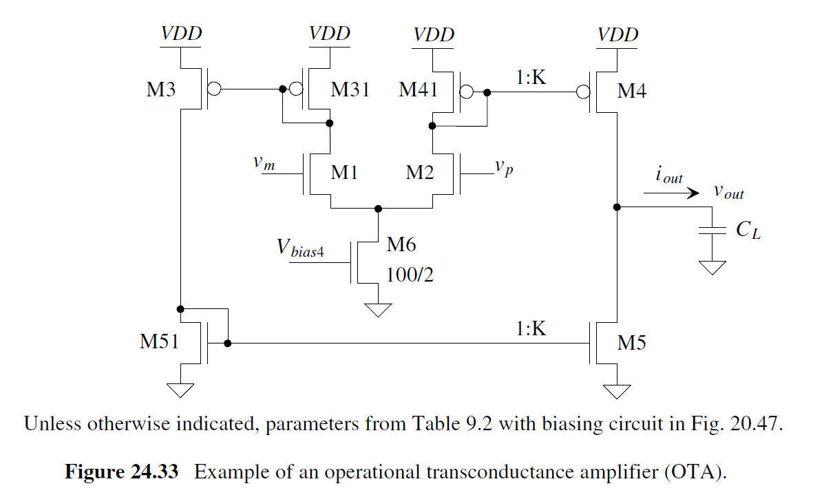
Voltage Gain:
A
v
=
v
o
u
t
v
p
−
v
n
=
K
⋅
g
m
⋅
(
r
o
4
∥
r
o
5
)
A_{v}=\frac{v_{out}}{v_{p}-v_{n}}=K\cdot g_{m}\cdot \left( r_{o4}\parallel r_{o5} \right)
Av=vp−vnvout=K⋅gm⋅(ro4∥ro5)
OTA gm:
g
m
O
T
A
=
i
o
u
t
v
p
−
v
n
=
K
⋅
g
m
g_{mOTA}=\frac{i_{out}}{v_{p}-v_{n}}=K\cdot g_{m}
gmOTA=vp−vniout=K⋅gm
unity-gain frequency:
f
u
n
=
g
m
n
2
π
C
L
=
24
M
H
z
f_{un}=\frac{g_{mn}}{2\pi C_{L}}=24MHz
fun=2πCLgmn=24MHz
Dominant Pole:
f
3
d
B
=
1
2
π
(
r
o
4
∥
r
05
)
C
L
=
1.4
M
H
z
f_{3dB}=\frac{1}{2\pi \left( r_{o4}\parallel r_{05} \right)C_{L}}=1.4MHz
f3dB=2π(ro4∥r05)CL1=1.4MHz
Note that the maximum value of iout is KIss, 这里和之前slew-rate Limitation时增大了K倍.
Increasing the OTA Output Resistance
为了增大OTA输出阻抗, 可采用casecode结构
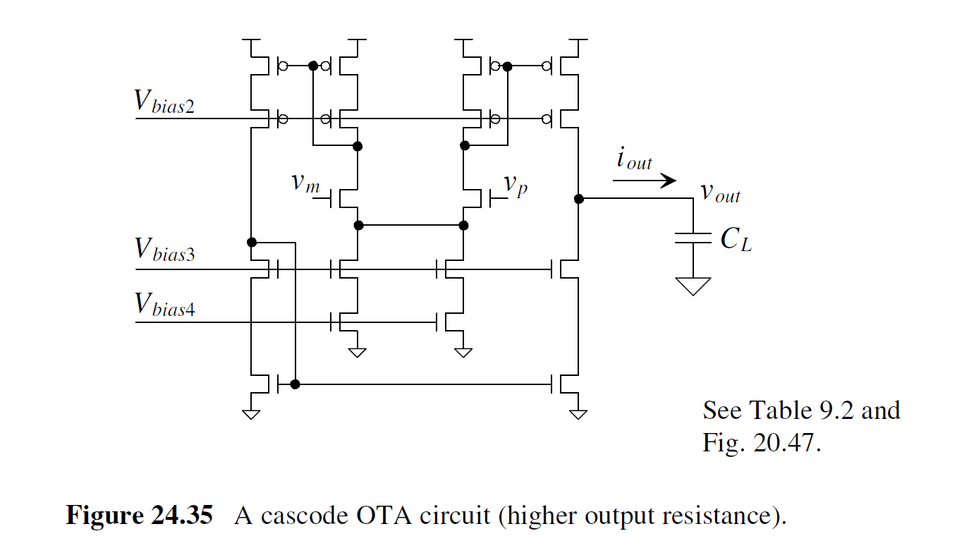
A
v
=
g
m
n
⋅
(
R
o
c
a
s
n
∥
R
o
c
a
s
n
)
=
500
(
54
d
B
)
A_{v}=g_{mn}\cdot \left( R_{ocasn}\parallel R_{ocasn} \right)=500 (54dB)
Av=gmn⋅(Rocasn∥Rocasn)=500(54dB)
f 3 d B = 1 2 π ( R o c a s n ∥ R o c a s n ) ⋅ C L = 47 K H z f_{3dB}=\frac{1}{2\pi \left( R_{ocasn}\parallel R_{ocasn} \right) \cdot C_{L}}=47KHz f3dB=2π(Rocasn∥Rocasn)⋅CL1=47KHz
An Important Note
与两级运放不同, 增加输出电容会让OTA更加稳定, Phase Margin更接近90.
In many on-chip applications, the load is purely capacitive and so the OTA works great as an “op-amp” in a closed-loop configuration (thus we’ll often call OTAs op-amps).
在芯片内部, 负载就是纯电容, 因此在芯片内部closed-loop design中OTA视为很好的op-amp
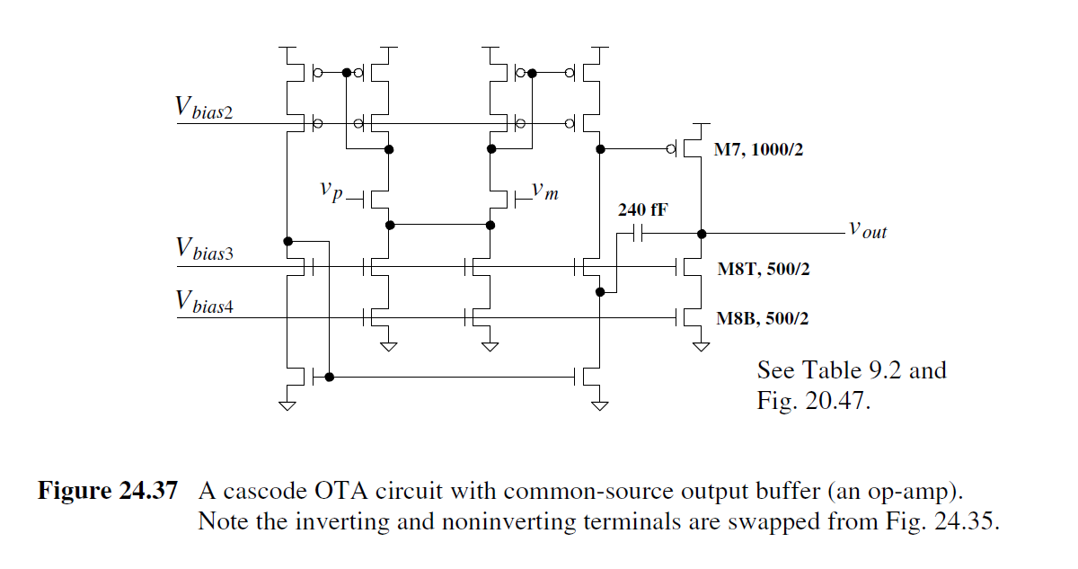
OTA with an Output Buffer (An Op-Amp)
为了drive resistive load, 可以在OTA加入buffer,如下图所示
注意: 这种结构也是indirect feedback, 确保Cc反馈点和第二级的gate同一方向变化.
或者加入Class-AB output stage
注意: 这种结构也是indirect feedback, 确保Cc反馈点和第二级的gate同一方向变化.
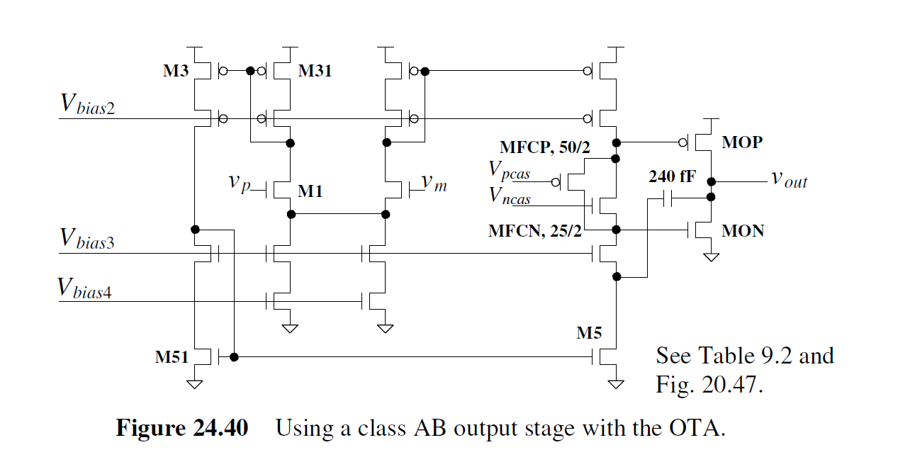

Fig 24.40比起Fig24.29, 其step response要差一些. 原因在于 Fig 24.40的vp传到vout需要经过 ( M1 - M31 - M3 - M51 - M5 - MON). The delay through this path is longer than the delay, in Fig. 24.29, through M2 - MOP. Fig 24.40输入信号传递的路径长.
Further, for high speed, M5 of the op-amp in Fig. 24.40 must turn on to pull the gate of MON down. For the op-amp in Fig. 24.29, the fact that both the gate of M9T and MOP are driven (in opposite directions) by the diff-amp allow us to use a simple pull-down current (M8) without losing speed.
Fig 24.29的潜在问题是limited input common-mode range and the limited voltage swing of node 1. Towards getting better input common-mode voltage range and output swing as well as improved high-speed operation, let’s discuss the folded-cascode OTA.
The Folded-Cascode OTA and Op-Amp
为了解决Fig 24.29的输入共模电平和节点1的摆幅问题, 我们引入folded-cascode OTA:
请注意电流Bias的大小.
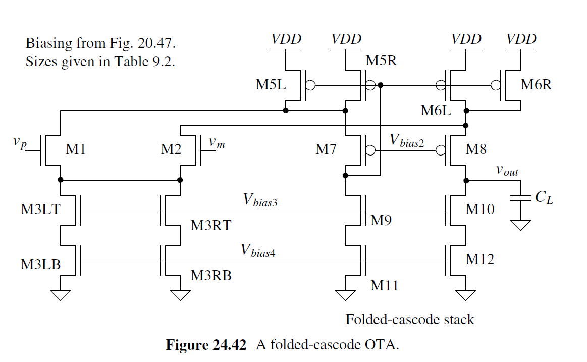
定性工作原理分析: vp上升, M5 drain下降, M7 off, M5 gate下降, M6电流上升, M2 off, M8 source变大, M8电流变大, Vout上升.
这个OTA最多能source 20uA, 最大能sink 10uA电流
该OTA为单极点系统:
A
v
=
g
m
n
⋅
(
R
o
c
a
s
n
∥
R
o
c
a
s
n
)
A_{v}=g_{mn}\cdot \left( R_{ocasn}\parallel R_{ocasn} \right)
Av=gmn⋅(Rocasn∥Rocasn)
Folded-cascode op-amp using a class AB output buffer 如下图所示
floating current sources to equalize the voltages across M9/M10 (to minimize the input-referred offset). 在M9和M10上加floating current source.
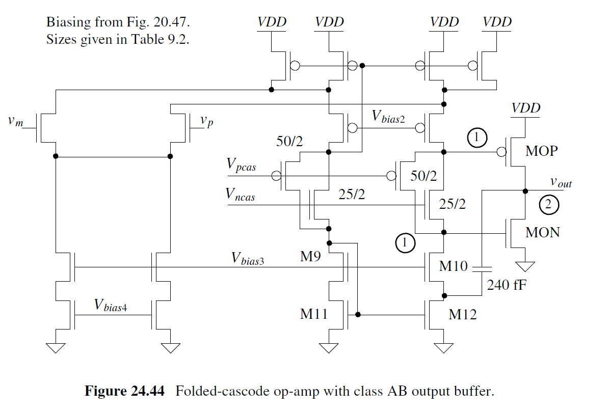
这个folded-cascde+ class AB架构 step-response一般.
We can’t seem to push the gain-bandwidth product, much above 100 MHz. Again, the only way to increase the speed is to reduce the channel length and/or increase the overdrive voltage.
GBW我们改善不了, 提高step response响应速度只能减小L或者增加override voltage (让Vgs-Vth更大)
加入PMOS Input Pairs, 让input common-mode voltage extends beyond the power supply rail的folded-casecode如下图所示
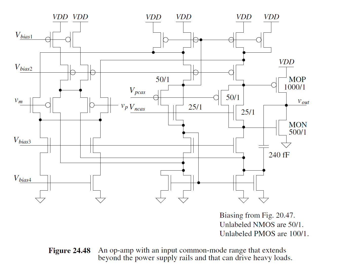
注意gm会随着输入电压变化而变化
注意: 对于有些应用Class AB的输出电流需要很大, 例如100mA. 这会造成op-amp的quiescent current达到1mA. 为了降低op-amp功耗, 我们只能把floating current sources的L变大, 即W/L变小, 这会导致floating current sources的Vgs变大, 导致push-pull 管子的Vgs更小 (shutting them off) , 因为Vgs (floating) + Vgs (push-pull) = Vbias (constant). 这会导致第二级的gm2 变小, 由下面公式Eq 24.24 可知, 会导致次级点f2 变小, thus making the op-amp unstable. 对于需要输出大电流的Class-AB设计不易啊.
f
1
=
1
2
π
g
m
2
R
2
R
1
C
c
f_{1}=\frac{1}{2\pi g_{m2}R_{2}R_{1}C_{c}}
f1=2πgm2R2R1Cc1
f 2 = g m 2 C c 2 π C 1 ( C L + C c ) f_{2}=\frac{g_{m2}C_{c}}{2\pi C_{1}(C_{L}+C_{c})} f2=2πC1(CL+Cc)gm2Cc
Gain-Enhancement
对于GBW=AOLDC*f3db
我们可以采用Gain-Enhancement (GE)技术来增加DC-Gain, 以弥补L=1时gain的loss.
首先介绍一下我们在GE中用到的diff-amp with source-follower. 其作用就是转换输入电平, PMOS对input可接近GND, NMOS对input可接近VDD.
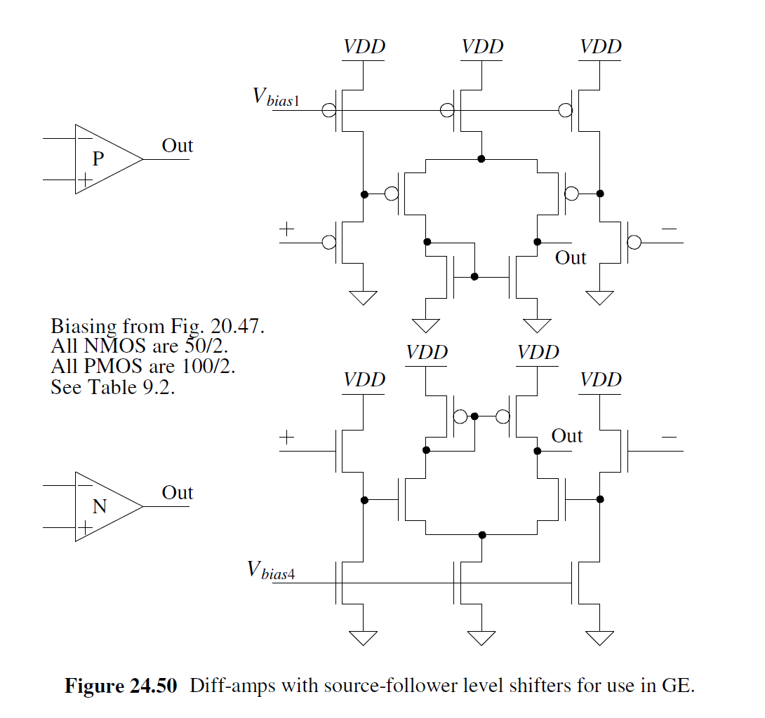
改造Fig24.44后的Folded-cascode op-amp with class AB output buffer and gain-enhancement 如下图所示:
GE的主要作用是钳位casecode 镜像管子的VDS相同, 确保current mirror match更好.
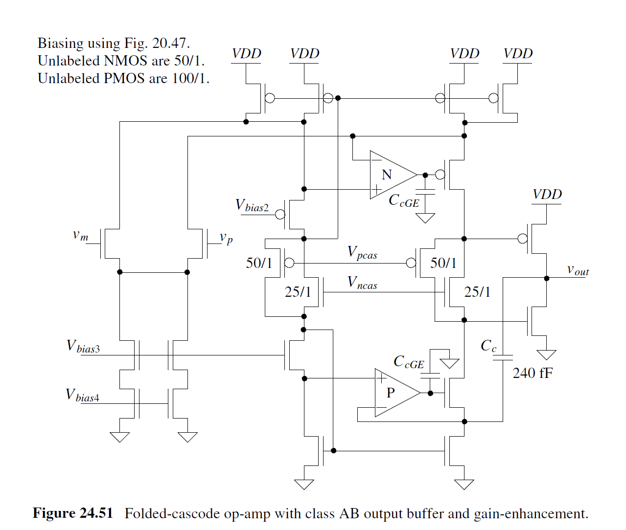
没有GE dc gain=53dB. 加入GE DC Gain=74dB
Bandwidth of the Added GE Amplifiers
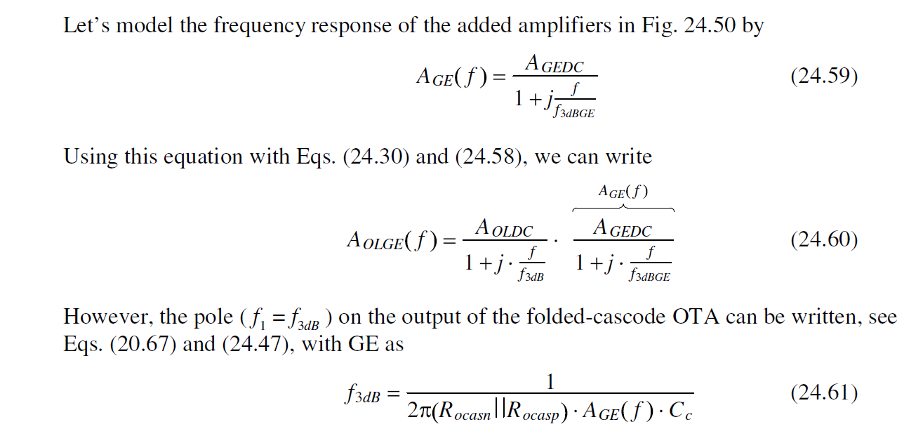
注意the bandwidth of the added amplifiers doesn’t need to be wide. As long as the bandwidths are larger than the f3dB of the op-amp.
GE op-amp的GBW不需要太大, 只需要大于原始op-amp的f3dB (first pole)就行了.
the resulting transfer function shows a doublet (a pole and zero at the same frequency). If the pole and zero aren’t at exactly the same frequency, then the settling time of the amplifier can be affected by the change in phase shift.
把Eq.24.61带入Eq24.60产生了doublet(零极点对), 这会影响op的setting time.
Compensating the Added GE Amplifiers
为了系统稳定性, 可以在GE输出加入CcGE=240 fF (GE OTAs GBW=100 MHz), 因为GE的GBW不需要很大, 系统step response性能更好.
Some Examples and Discussions
A Voltage Regulator
A voltage reference is used with the op-amp to generate a regulated voltage, VREG.
采用OP和基准产生想要的电压基准.
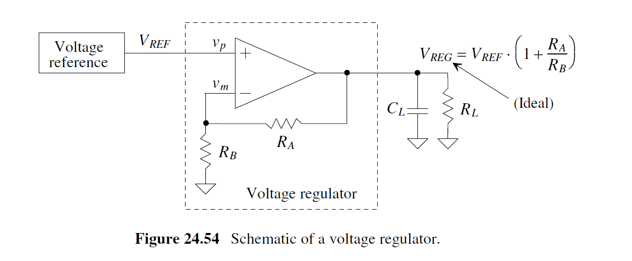
OP Open-Loop gain infinite:
V
R
E
G
=
V
R
E
F
(
1
+
R
A
R
B
)
V_{REG}=V_{REF}\left( 1+\frac{R_{A}}{R_{B}} \right)
VREG=VREF(1+RBRA)
Op with finite open-loop gain:
V
R
E
G
=
V
R
E
F
1
1
A
O
L
+
R
B
R
A
+
R
B
V_{REG}=V_{REF}\frac{1}{\frac{{1}}{A_{OL}}+\frac{R_{B}}{R_{A}+R_{B}}}
VREG=VREFAOL1+RA+RBRB1
This is why open-loop gain is important. 直接影响输出精度.
下图所示用两级Op-amp搭了一个Voltage Regulator.
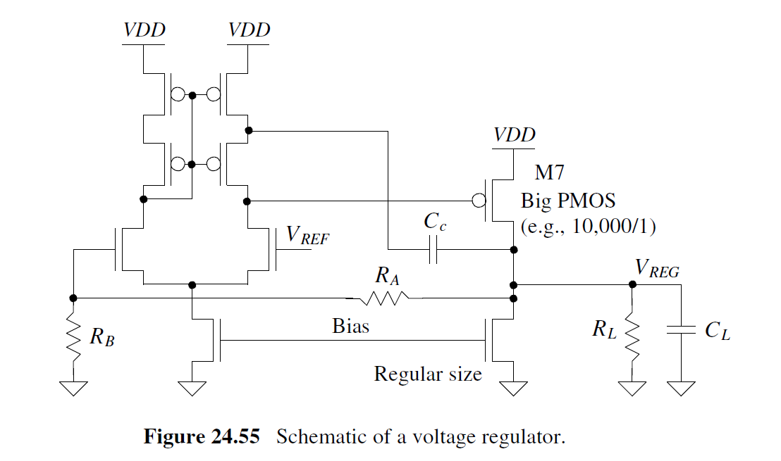
为了提供较大current source, M7 size较大, 当然这会带来offset.
还有一个问题是M7 gate最小电压 = VREF - Vthn (为了保证输入input in Saturation). 我们希望M7的gate能拉到GND.
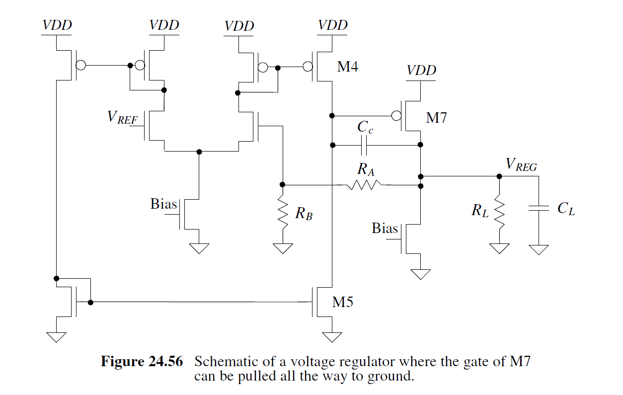
于是我们用Fig 24.33介绍的symmetric OTA搭了个Voltage Regulator, 如下图所示. 这样M7的gate就能拉到GND了, 允许M7 fully turn on.
Voltage Regulator - LDO稳定性的讨论
在实际使用中, 为了supply load transient和输出电压稳定性, Vreg处会放较大bypass capacitor (CL) 作为filter cap.
但是按照前面讨论, first pole在M7 gate处, second pole在输出Vreg (pole-spliting). 如果CL变大, second pole会变小, 可能造成环路稳定性问题.
为了解决稳定性, 我们可以放一个NMOS source-follower (SF) between the load and the output of the second stage. 但问题是我们可能没办法bias SF这么多current.
we must try to compensate the op-amp with the load capacitance. 我们需要想办法用CL来补偿op-amp, 即把dominant pole放在CL. 因此需要设置CL_min, CL越大系统越稳定.
问题: 既然把dominant pole放在CL, 为什么还需要Cc (Cc pole-splitting只会让1st pole更大, 更不稳定)?
原因: Cc能帮助large-signal, 如果Vreg drop, 通过Cc M7 gate也drop, M7 on提供更大电流补偿Vreg Drop.
Cc并不是为了补偿稳定性, 相反会让稳定性更差, 另外增大first-stage的gain, 会增大first-stage output resistance R1, 也会影响稳压系统稳定性.
计算output pole (dominant pole)
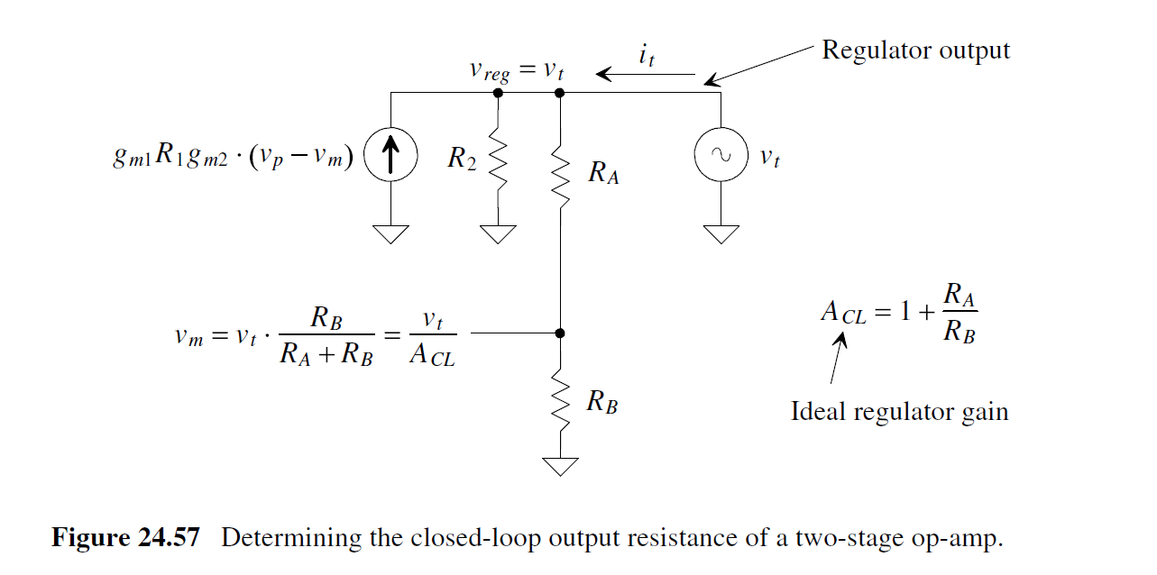
输出电阻, 注意带负反馈的Rout 减小了Aoldc倍
R
o
u
t
,
C
L
=
A
C
L
A
O
L
D
C
⋅
R
2
R_{out,CL}=\frac{A_{CL}}{A_{OLDC}}\cdot R_{2}
Rout,CL=AOLDCACL⋅R2
A C L = 1 + R A R B A_{CL}=1+\frac{R_{A}}{R_{B}} ACL=1+RBRA
Output pole:
f
2
=
1
2
π
R
o
u
t
,
C
L
C
L
⋅
A
C
L
=
A
O
L
D
C
2
π
R
2
C
L
⋅
A
C
L
f_{2}=\frac{1}{2\pi R_{out,CL}C_{L}\cdot A_{CL} }=\frac{A_{OLDC}}{2\pi R_{2}C_{L}\cdot A_{CL}}
f2=2πRout,CLCL⋅ACL1=2πR2CL⋅ACLAOLDC
为了减少output pole, AOLDC需要减小, 另外note1的resistance不要太大, 但Aoldc小会导致regulation精度变差.
另外注意ACL=(RA+RB)/RB, 因此unity gain buffer的ACL最小, 最难补偿.
M7 gate处的pole (假设Cgs7 >> Cc)
f
1
=
1
2
π
R
1
C
g
s
7
f_{1}=\frac{1}{2\pi R_{1}C_{gs7}}
f1=2πR1Cgs71
We want f2<< f1
f
u
n
=
A
O
L
D
C
⋅
f
2
=
A
O
L
D
C
2
2
π
R
2
C
L
m
i
n
⋅
A
C
L
f_{un}=A_{OLDC}\cdot f_{2}=\frac{A_{OLDC}^{2}}{2\pi R_{2} C_{Lmin}\cdot A_{CL}}
fun=AOLDC⋅f2=2πR2CLmin⋅ACLAOLDC2
由于片上系统, CL不能太大. 另外假设M7, RL<<ro7, 另外M7的output resistance dominates R2
C
L
m
i
n
R
L
m
a
x
=
(
g
m
1
R
1
g
m
2
)
2
2
π
⋅
f
u
n
⋅
A
C
L
\frac{C_{Lmin}}{R_{Lmax}}=\frac{(g_{m1}R_{1}g_{m2})^{2}}{2\pi\cdot f_{un}\cdot A_{CL}}
RLmaxCLmin=2π⋅fun⋅ACL(gm1R1gm2)2
If we select CLmin=1000pF, then RLmax=1k. RLmax代表LDO能稳定的最小负载.
We might think, after looking at f2 equation, that by supplying more current (RL or R2 decreasing further), the location of f2 increases and the regulator moves towards instability. However, for further decreases in the load resistance, the current supplied by M7 increases and thus so does its gm. What happens is this: we get the canceling of effects. As the current supplied to the output increases linearly with a linear decrease in RL , the value of gm^2 increases linearly and the effects cancel.
看到f2的公式, 我们可能会想增加M7电流能减小RL或者R2值, 导致f2变大, 导致LDO不稳定. 但其实不会, 增加负载电流会导致M7的gm变大, gm^2变大, cancel这个effect.
这个LDO design和我们之前设计不同, 需要在PVT全Corner下验证其稳定性.
Bad Output Stage Design
In this section we’ll discuss some problems with biasing in Class AB output stages.
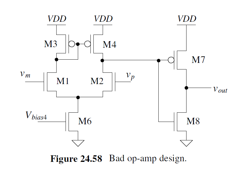
上图的问题是 push-pull的电流不由bias circuit决定, 电流能变化极大. The problem is that the current flowing in the push-pull output stage (an inverter) isn’t set by a bias circuit.
还有一个问题是, M8的gate=VDD-Vsg. Keep M8 in Saturation, Vout需要>=VDD-Vsg-Vthn. 限制了Vout output swings.
于是我们加一个source follower来降低M8的gate voltage.如下图所示.
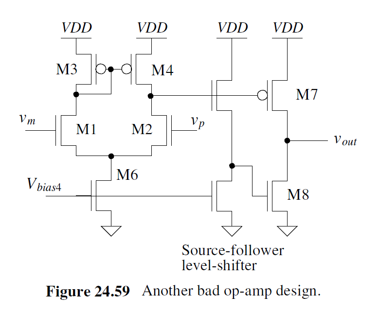
但是Fig 24.59问题还是不能控制output stage current. input offset=10mV, gain=20, 那么M7,M8 gate上的变化能达到200mV, 导致M7/M8的电流变化上百uA.
为了精准控制输出电流, 考虑下图结构.
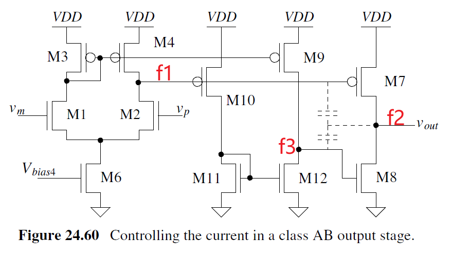
我们treat M4 drain=M3 gate, 因此M7, M10, M9的gate和电流相等. 我们treat M8 gate=M11 gate. 因此ID_M7=ID_M8. 我们貌似解决了Class AB的电流偏置问题.
但问题是我们有三个高阻节点. f1, f2和f3. 如果我们把f1作为dominant pole, 其他pole没有受影响. then the path that the op-amp inputs sees through M3 to M9 to the gate of M8 (the other high-impedance node) isn’t affected.
如果我们在f1,f2,f3上加补偿电容, 电流不一定能保持平衡.
If we add compensation capacitors from the op-amp output to both the gates of M7 and M8, the current fed back isn’t necessarily balanced. 主要是影响large signal的setting time和stability.
即便如此, 这个topology在低功耗和低VDD下还是有用的.
为了简化电路, 我们可以把M12 diode connected, 去掉M10/M11. 那么这就不再是class AB了. M9 mirror M3, 电流流向M12, M8 mirror M12.
Three-Stage Op-Amp Design
当需要设计low power-supply voltage or with minimal power from VDD. class AB output stage需要的VDD_min较高就用不了. 我们仍然需要用用两级或者三级运放.
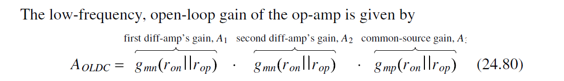
考虑下图的three-stage op-amp. This design is a cascade of two diff-amps followed by a common-source amplifier. 两个diff串联CS.
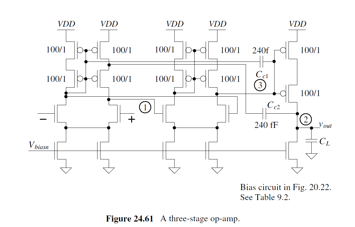
three-stage op-amp的难题在于compensation. 我们仍然希望node1为dominant pole. 上图的nesting of the compensation 也称为 nested Miller compensation (当然实际上我们用了indirect feedback compensation)
Note how the current through Cc1 feeds back to node 1 through the diode-connected load of the input diff-amp. This is necessary to ensure that the signal through Cc1 adds with the signal fed back directly to node 1 through Cc2.
由于pole-splitting, node3的pole为
f
3
=
g
m
n
2
π
C
1
f_{3}=\frac{g_{mn}}{2\pi C_{1}}
f3=2πC1gmn
gmn为第二级diff-amp的transconductance, 并且C1>>第三级CS的input cap
The location of the pole on the output:
f
2
=
g
m
p
⋅
C
c
2
2
π
⋅
C
1
(
C
L
+
C
c
2
)
f_{2}=\frac{g_{mp}\cdot C_{c2}}{2\pi\cdot C_{1}(C_{L}+C_{c2})}
f2=2π⋅C1(CL+Cc2)gmp⋅Cc2
GBW:
f
u
n
=
G
B
W
=
g
m
n
2
π
(
C
c
2
+
C
c
1
/
A
3
)
=
g
m
n
2
π
C
c
2
f_{un}=GBW=\frac{g_{mn}}{2\pi (C_{c2}+C_{c1}/A_{3})}=\frac{g_{mn}}{2\pi C_{c2}}
fun=GBW=2π(Cc2+Cc1/A3)gmn=2πCc2gmn
注意这里的gmn是第三级的gain.
Here, we’ll set Cc2 to 240 fF to get a unity-gain frequency of 100 MHz. We still need Cc1 to push node 3’s pole to a higher frequency (pole splitting). We’ll also set Cc1 to 240 fF.
If we drive a load capacitance, then we expect the third-stage gain, A3 , to start to decrease at a lower frequency (it starts to decrease sooner with increasing frequency). we then expect fun to drop in value.
输出加入负载电容, A3 gain减少, fun也会减小, 系统Phase Margin恶化. 为了解决稳定性问题, 我们可以增大Cc2来减小GBW, 来保持稳定.
最后讨论: 为什么我们要采用Fig24.61 两级diff-amp+一级Common Source这样的架构?
如果我们第二级用common source替代diff-amp, 我们将没办法确定第二级输出电压来bias第三级电流. 对于common-source放大器, 输出是未知的. without feedback to set it, is unknown (the two drains of the NMOS and PMOS will either float up or float down, depending on which device is sourcing or sinking the most current). 但是我们若采用diff-amp, 输出电压和bias电流能确定.如下图所示.
我们输出级不用diff-amp是因为限制呢output摆幅, diff-amp’s limited output swing.
另外两级diff-amp极大增加了CMRR, 一级diff-amp的CMRR是80dB, 两级就是160dB. Another benefit of using two diff-amps on the input of he op-amp is the increase in the CMRR.


 2252
2252

 被折叠的 条评论
为什么被折叠?
被折叠的 条评论
为什么被折叠?
 到【灌水乐园】发言


