


 本文详细介绍了CycloneIVE集成电路的I/O银行布局,强调了差分信号标准如LVDS、RSDS在特定行的支持,以及GPIO的灵活性。还讨论了LVPECL、HSTL和SSTL标准在时钟输入和PLL输出的应用,以及阻抗匹配的重要性。
Ps.1:
Cyclone IV E I/O Banks
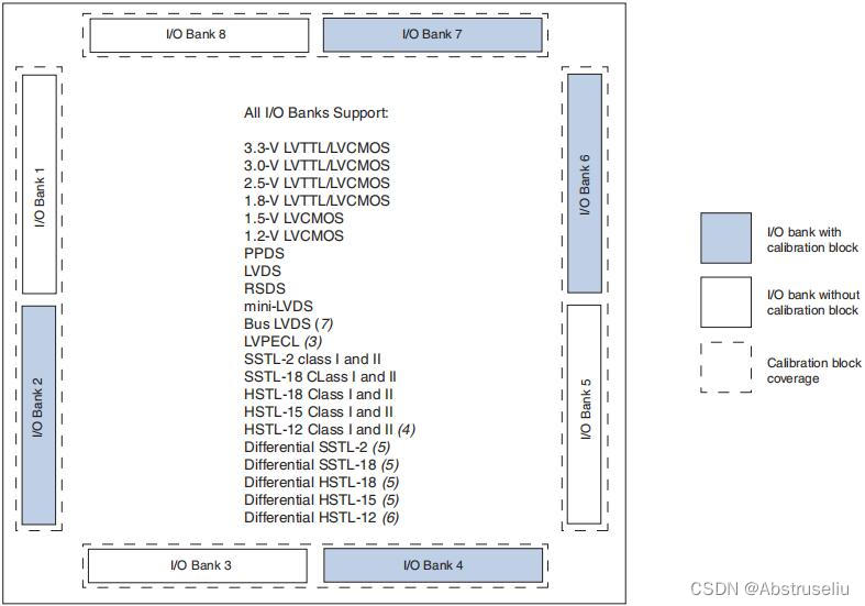
Notes to Figure 6–9:
(1)This is a top view of the silicon die. This is only a graphical representation. For exact pin locations, refer to the pin list and the QuartusII software.
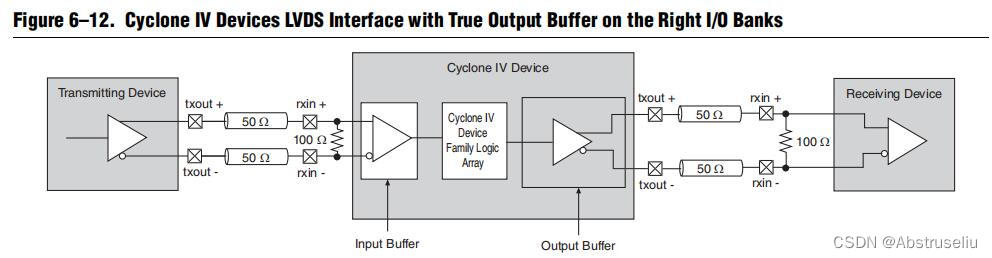
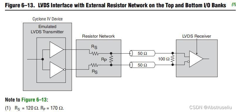
(2)True differential (PPDS, LVDS, mini-LVDS, and RSDS I/O standards) outputs are supported in row I/O banks 1, 2, 5, and 6 only. External resistors are needed for the differential outputs in column I/O banks.
(3)The LVPECL I/O standard is only supported on clock input pins. This I/O standard is not supported on output pins.
(4)The HSTL-12 Class II is supported in column I/O banks 3, 4, 7, and 8 only.
(5)The differential SSTL-18 and SSTL-2, differential HSTL-18, and HSTL-15 I/O standards are supported only on clock input pins and phase-locked loops (PLLs) output clock pins. Differential SSTL-18, differential HSTL-18, and HSTL-15 I/O standards do not support Class II output.
(6)The differential HSTL-12 I/O standard is only supported on clock input pins and PLL output clock pins. Differential HSTL-12 Class II is supported only in column I/O banks 3, 4, 7, and 8.
(7)BLVDS output uses two single-ended outputs with the second output programmed as inverted. BLVDS input uses true LVDS input buffer.
译为:
(1)这是硅模具的俯视图。这只是一个图形表示。有关准确的引脚位置,请参考引脚列表和Quartus II软件。
(2)仅在I/O行1、2、5和6行中支持真差分(PPDS、LVDS、mini-LVDS和RSDS I/O标准)输出。列I/O组的差分输出需要外部电阻。
(3)LVPECL输入/O标准只支持时钟输入引脚。输出引脚不支持此I/O输出标准。
(4)HSTL-12第3类II类、只支持第3、4、7、8栏。
(5)差动SSTL-18和SSTL-2、差动HSTL-18和HSTL-15 I/O标准仅支持时钟输入针脚和锁相环(PLLs)输出时钟针脚。差分SSTL-18、差分HSTL-18和HSTL-15 I/O标准不支持II类输出。
(6)差分HSTL-12 I/O标准只支持时钟输入引脚和PLL输出时钟引脚。差分HSTL-12II类仅支持列I/O组3、4、7和8。
(7) BLVDS输出使用两个单端输出,第二个输出被编程为反向输出。BLVDS输入使用真正的LVDS输入缓冲区。
Ps.2:
Designing with LVDS
为什么Bank不同阻抗匹配方式不同?
Ps.3:GPIO(英语:General-purpose input/output),通用型之输入输出的简称,功能类似8051的P0—P3,其接脚可以供使用者由程控自由使用,PIN脚依现实考量可作为通用输入(GPI)或通用输出(GPO)或通用输入与输出(GPIO),如当clk generator, chip select等。既然一个引脚可以用于输入、输出或其他特殊功能,那么一定有寄存器用来选择这些功能。对于输入,一定可以通过读取某个寄存器来确定引脚电位的高低;对于输出,一定可以通过写入某个寄存器来让这个引脚输出高电位或者低电位;对于其他特殊功能,则有另外的寄存器来控制它们。
Ps.4:RSDS reduced swing differential signal 低摆幅差分信号
由于平板显示器的画面越来越大,因此更简单的设计及更低的功耗显得更为重要,对于笔记本型计算机及其他便携式设备来说,其重要性尤其不能忽视,因为这些产品必须外型轻巧幼薄,不能为了提高清晰度及降低元件数目而牺牲这两方面的优势。
采用 RSDS 技术亦可为新一代的显示器产品添加更多重要的功能特色及优点。例如,可大幅节省用电量而无损其性能及分辨率。对于以电池供电及便携式的系统来说,这个优点显得尤为重要。由电磁干扰引起的噪音也因此而可以大幅减少,使生产成本得以降低,而产品亦可以更快推出市场。


 418
418

 被折叠的 条评论
为什么被折叠?
被折叠的 条评论
为什么被折叠?
 到【灌水乐园】发言


