


eMMC特性初探–基于eMMC spec v5.1
- 以下是基于eMMC 5.1 Spec Chapter1~Chpater5 整理的基本特性。 后续会整理其他章节的内容。
1.eMMC System Features:
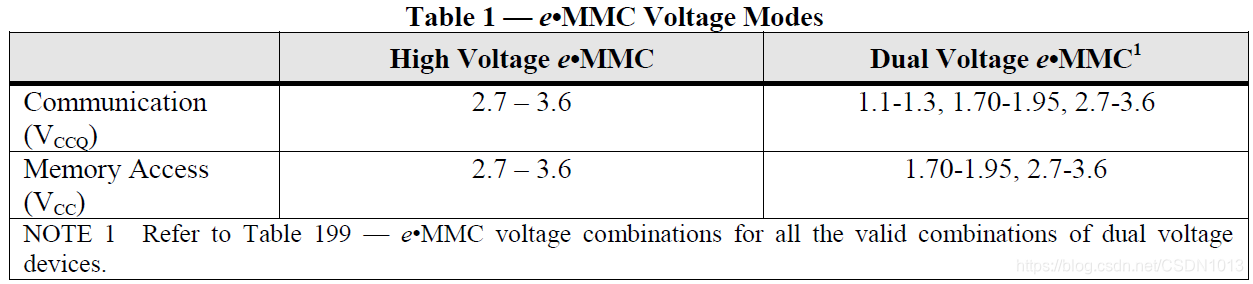
1.1 System Voltage (VCC and VCCQ) Ranges (Table 1).
1.2 Eleven-wire bus (clock, Data Strobe, 1 bit command, 8 bit data bus) and a hardware reset.
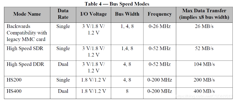
1.2.1 Clock frequencies of 0-200MHz
1.2.2 Three different data bus width modes: 1-bit (default), 4-bit, and 8-bit
1.2.3 Data protection Mechanisms :
- Password
- Permanent
- Power-On
- Temporary
1.2.4 Different types of error protected read and write modes:
- Single Block
- Multiple Block
1.2.5 Data Removal Commands:
- Erase
- Trim
- Sanitize
1.2.6 Protection methods for data during sudden power failures
1.2.7 Capability for customized solutions using application specific commands
1.2.8 Power Saving Sleep mode
1.2.9 Boot Areas that will automatically stream data when using defined boot modes.
1.2.10 Signed access to a Replay Protected Memory Block.
1.2.11 Two types of high capacity devices: small 512B sector devices and large 4KB sector devices.
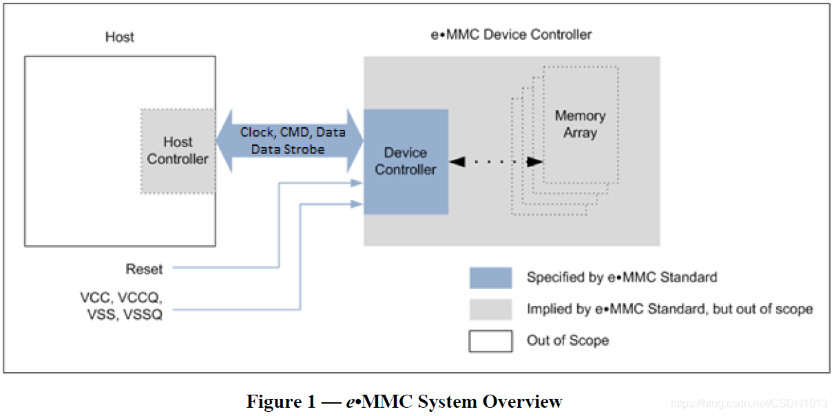
2. e•MMC Device and System Diagram
2.1 内存寻址:
2.1.1 eMMC 4.1的寻址位数最大为8byte,导致eMMC的最大容量为2GB。
2.1.2 eMMC 5.1 支持sector address(512B sectors). The sector addresses shall be used for all devices with capacity larger than 2 GB. Host应该读取OCR寄存器的[30:29]bit,来决定寻址模式。
2.2 信号概述:
请参考下面的表格: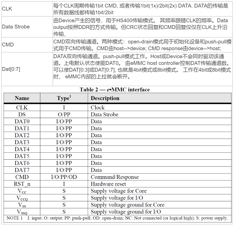
2.3 Information registers

Note: The host may reset the device by:
- Switching the power supply off and back on. The device shall have its own power-on detection circuitry that puts the device into a defined state after the power-on.
- A reset signal
- By sending a special command
3. 总线协议
3.1 Overview:
上电reset后,host必须初始化device. Host通过CID识别设备。 CID的24bit寄存器包括MID和OID。每个设备出厂前都会设置唯一的MID。这是由JEDEC规定的。
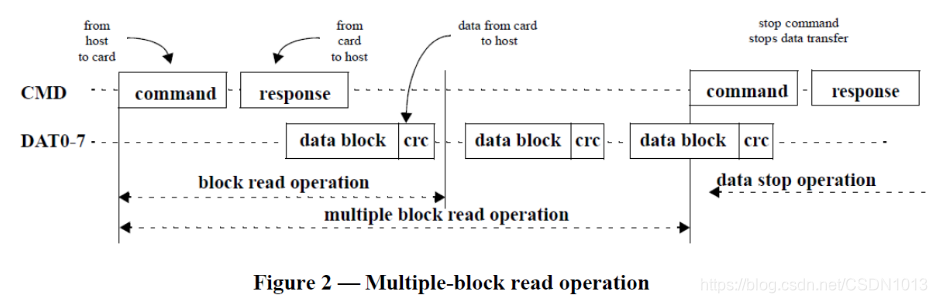
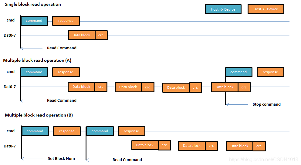
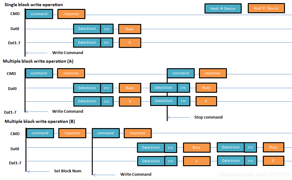
3.2 读写操作概述
读和写都是按照block为单位。读和写都可以是single block或者multiple block. 读、写数据时,都会跟CRC。A multiple block transmission is terminated when a stop command follows on the CMD line similarly to the sequential read.
- A simple busy signaling of the write operation duration on the data (DAT0) line is used.
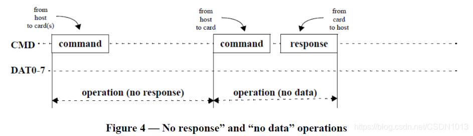
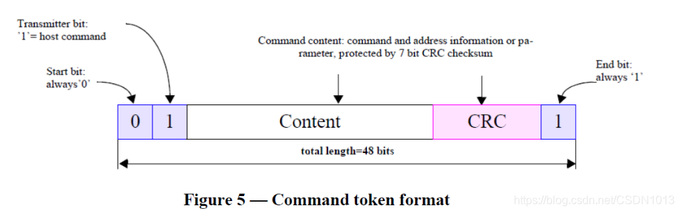
3.3 CMD部分详述:
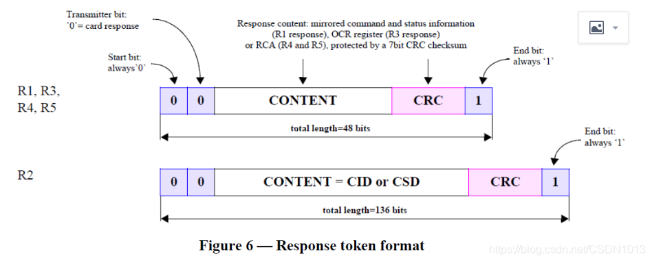
3.4 Response部分详述:
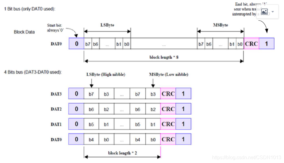
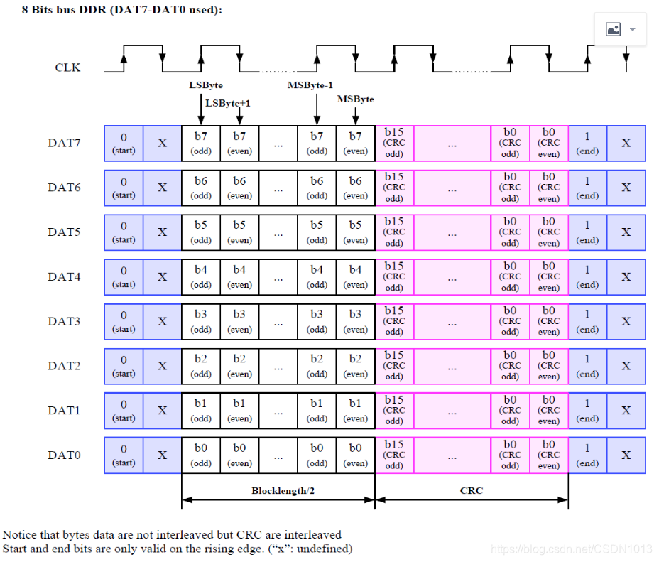
3.5.1 Data部分详述(SDR):

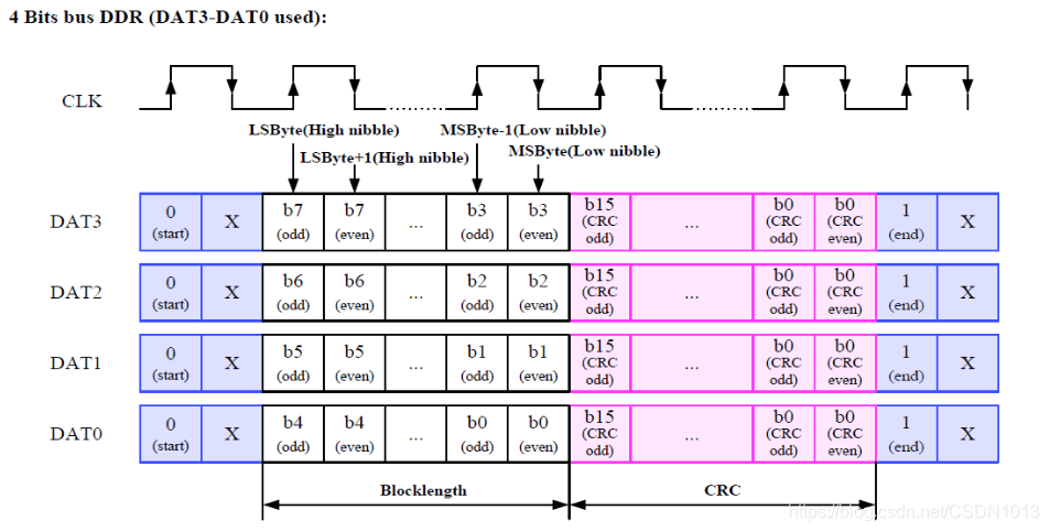
3.5.2 Data部分详述(DDR):
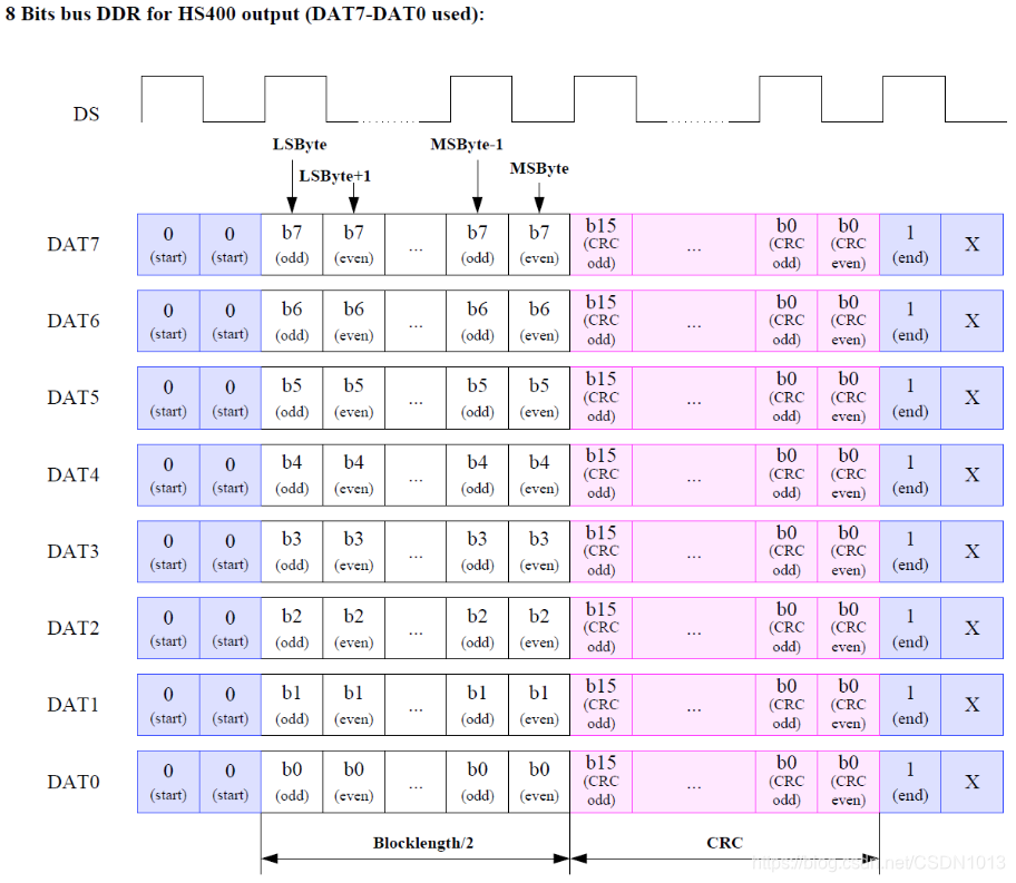
3.6 HS200 mode features VS HS400 mode features
- 基本特性
- 其他特性
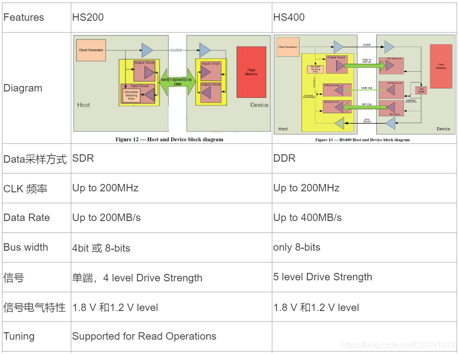
- HS200 Block diagram: Host产生CLK,用于传输的同步。写操作时,CLK和DAT的传输方向相同(Host–>Device), 所以即使有传输线延迟的情况下DAT write也可以与CLK同步。读操作时,CLK与DAT传输方向相反。Host接收DAT的延迟来源有: Round-trip delay(来回通讯延迟),Output delay(输出延迟)和主从之间的延迟。
- 为了解决读操作的不同步问题,the Host needs to have an adjustable sampling point to reliably receive the incoming data. Host可以使用Device端预置的tuning block,来寻找optimal sampling point。Host可以通过CMD21访问tuning block。
- HS400 Block Diagram: 同样由Host产生CLK。与HS200不同的是, HS400模式中,Device端输出DS信号,而data, CRC status,CMD response(当使能enhanced strobe时)与DS边沿对齐。 Host通过DS信号解决延迟问题。


 5451
5451

 被折叠的 条评论
为什么被折叠?
被折叠的 条评论
为什么被折叠?
 到【灌水乐园】发言


