


 Buck-Boost转换器是一种DC-DC转换器,其输出电压可以大于或小于输入电压。它通过开关器件和电感实现升压或降压效果。转换器有两种工作模式:当开关导通时,电流流经电感并储存能量;当开关断开时,电感释放储存的能量,通过负载和二极管维持电流方向。通过脉宽调制(PWM)控制开关的占空比,可以调整输出电压。当占空比D大于0.5时,输出电压高于输入;反之则低于输入。
July 25, 2021 by Electrical4U

What is a Buck Boost Converter?
The buck–boost converter is a type of DC-to-DC converter (also knownas a chopper) that has an output voltage magnitude that is either greater than or less than the input voltage magnitude. It is used to “step up” the DC voltage, similar to a transformer for AC circuits.
It is equivalent to a flyback converter using a single inductor instead of a transformer. Two different topologies are called buck–boost converter.
DC-DC converters are also known as choppers. Here we will have a look at Buck Boost converter which can operate as a DC-DC Step-Down converter or a DC-DC Step-Up converter dependingupon the duty cycle, D.
A typical Buck-Boost converter is shown below.

The input voltage source is connected to a solid state device. The second switch used is a diode. The diode is connected, in reverse to the direction of power flow from source, to a capacitor and the load and the two are connected in parallel as shown in the figure above.
The controlled switch is turned on and off by using Pulse Width Modulation(PWM). PWM can be time based or frequency based.
Frequency based modulation has disadvantages like a wide range of frequencies to achieve the desired control of the switch which in turn will give the desired output voltage.
Time based Modulation is mostly used for DC-DC converters. It is simple to construct and use.
The frequency remains constant in this type of PWM modulation. The Buck Boost converter has two modes of operation. The first mode is when the switch is on and conducting.
Mode I : Switch is ON, Diode is OFF

The Switch is ON and therefore represents a short circuit ideally offering zero resistance to the flow of current so when the switch is ON all the current will flow through the switch and the inductor and back to the DC input source.
The inductor stores charge during the time the switch is ON and when the solid state switch is OFF the polarity of the Inductor reverses so that current flows through the load and through the diode and back to the inductor. So the direction of current through the inductor remains the same.
Let us say the switch is on for a time TON and is off for a time TOFF. We define the time period, T, as

and the switching frequency,

Let us now define another term, the duty cycle,

Let us analyse the Buck Boost converter in steady state operation for this mode using KVL.

Since the switch is closed for a time TON = DT we can say that Δt = DT.

While performing the analysis of the Buck-Boost converter we have to keep in mind that
- The inductor current is continuous and this is made possible by selecting an appropriate value of L.
- The inductor current in steady state rises from a value with a positive slope to a maximum value during the ON state and then drops back down to the initial value with a negative slope. Therefore the net change of the inductor current over any one complete cycle is zero.
Mode II : Switch is OFF, Diode is ON

In this mode the polarity of the inductor is reversed and the energy stored in the inductor is released and is ultimately dissipated in the load resistance and this helps to maintain the flow of current in the same direction through the load and also step-up the output voltage as the inductor is now also acting as a source in conjunction with the input source. But for analysis we keep the original conventions to analyse the circuit using KVL.
Let us now analyse the Buck Boost converter in steady state operation for Mode II using KVL.

Since the switch is open for a time.

we can say that.


It is already established that the net change of the inductor current over any one complete cycle is zero.

We know that D varies between 0 and 1. If D > 0.5, the output voltage is larger than the input; and if D < 0.5, the output is smaller than the input. But if D = 0.5 the output voltage is equal to the input voltage.
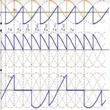
A circuit of a Buck-Boost converter and its waveforms is shown below.

The inductance, L, is 50mH and the C is 100µF and the resistive load is 50Ω. The switching frequency is 1 kHz. The input voltage is 100 V DC and the duty cycle is 0.5.

The voltage waveforms are as shown above and the current waveforms are as shown in the figure below.


 7万+
7万+

 被折叠的 条评论
为什么被折叠?
被折叠的 条评论
为什么被折叠?
 到【灌水乐园】发言


