


从芯片视角理解I2C Bus工作原理,转载自Texas Instruments Application report
Jonathan Valdez, Jared Becker
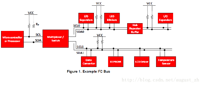
The I2C bus is a very popular and powerful bus used for communication between a master (or multiple masters) and a single or multiple slave devices. Figure 1 illustrates how many different peripherals may share a bus which is connected to a processor through only 2 wires, which is one of the largest benefits that the I2C bus can give when compared to other interfaces.
This application note is aimed at helping users understand how the I2C bus works.
Figure 1 shows a typical I2C bus for an embedded system, where multiple slave devices are used. The microcontroller represents the I2C master, and controls the IO expanders, various sensors, EEPROM, ADCs/DACs, and much more. All of which are controlled with only 2 pins from the master.
1 Electrical Characteristics
I2C uses an open-drain/open-collector with an input buffer on the same line, which allows a single data line to be used for bidirectional data flow.
1.1 Open-Drain for Bidirectional Communication
Open-drain refers to a type of output which can either pull the bus down to a voltage (ground, in most cases), or “release” the bus and let it be pulled up by a pull-up resistor. In the event of the bus being released by the master or a slave, the pull-up resistor (Rpu) on the line is responsible for pulling the bus voltage up to the power rail. Since no device may force a high on a line, this means that the bus will never run into a communication issue where one device may try to transmit a high, and another transmits a low, causing a short (power rail to ground). I2C requires that if a master in a multi-master environment transmits a high, but see’s that the line is low (another device is pulling it down), to halt communications because another device is using the bus. Push-pull interfaces do not allow for this type of freedom, which is a benefit of I2C.
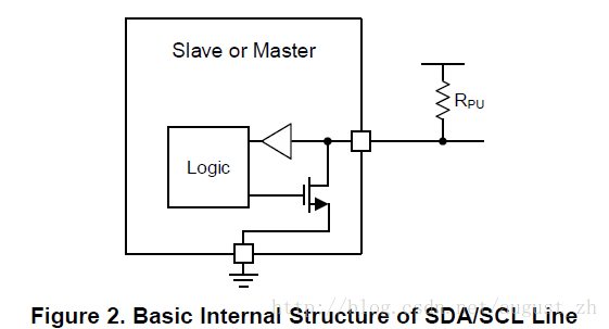
Figure 2 shows a simplified view of the internal structure of the slave or master device on the SDA/SCL lines, consisting of a buffer to read input data, and a pull-down FET to transmit data. A device is only able to pull the bus line low (provide short to ground) or release the bus line (high impedance to ground) and allow the pull-up resistor to raise the voltage. This is an inportant concept to realize when dealing with I2C devices, since no device may hold the bus high. This property is what allows bidirectional communication to take place.
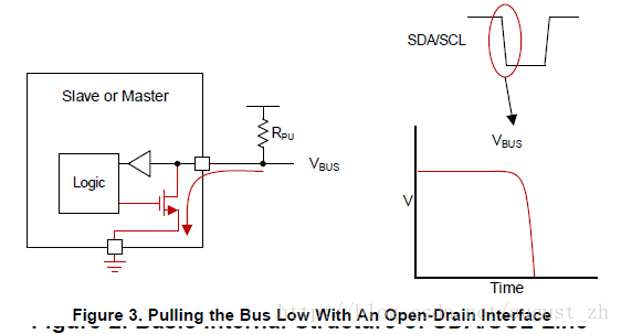
1.1.1 Open-Drain Pulling Low
As described in the previous section, the Open-Drain setup may only pull a bus low, or “release” it and let a resistor pull it high. Figure 2 shows the flow of current to pull the bus low. The logic wanting to transmit a low will activate the pull-down FET, which will provide a short to ground, pulling the line low.
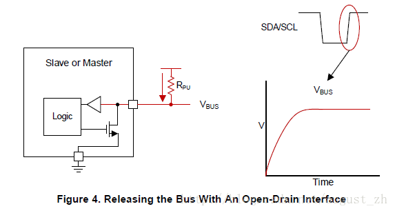
1.1.2 Open-Drain Releasing Bus
When the slave or master wishes to transmit a logic high, it may only release the bus by turning off the pull-down FET. This leaves the bus floating, and the pull-up resistor will put the voltage up to the voltage rail, which will be interpreted as a high. Figure 4 shows the flow of current through the pull-up resistor, which pulls the bus high.
2 I2C Interface
2.1 General I2C Operation
The I2C bus is a standard bidirectional interface that uses a controller, known as the master, to communicate with slave devices. A slave may not transmit data unless it has been addressed by the master. Each device on the I2C bus has a specific device address to differentiate between other devices that are on the same I2C bus. Many slave devices will require configuration upon startup to set the behavior of the device. This is typically done when the master accesses the slave’s internal register maps, which have unique register addresses. A device can have one or multiple registers where data is stored, written, or read.
The physical I2C interface consists of the serial clock(SCL) and serial data (SDA) lines. Both SDA and SCL lines must be connected to Vcc through a pull-up resistor. The size if the pull-up resistor is determined by the amount of capacitance on the I2C lines (for further details, refer to I2C pull-up Resistor calculation). Data transfer may be initiated only when the bus is idle. A bus is considered idle if both SDA and SCL lines are high after a STOP condition.
The general procedure for a master to access a slave device is the following:
(1) Suppose a master wants to send data to a slave:
- Master-transmitter sends a START condition and addresses the slave-receiver
- Master-transmitter sends data to slave-receiver
- Master-transmitter terminates the transfer with a STOP condition
(2) If a master wants to receive/read data from a slave:
- Master-receiver sends a START condition and addresses the slave-transmitter
- Master-receiver sends the requested register to read to slave-transmitter
- Master-recevier receives data from the slave-transmitter
- Master-receiver terminates the transfer with a STOP condition
2.1.1 STRAT and STOP Conditions
I2C communications with this device is initiated by the master sending a START condition and terminated by the master sending a STOP condition. A high-to-low transition on the SDA line while the SCL is high defines a STRAT condition. A low-to-high transition on the SDA line while the SCL is high defines a STOP condition.
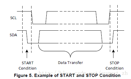
2.1.2 Repeated START Condition
A repeated START condition is similar to a START condition and is used in place of a back-to-back STOP then START condition. It looks identical to a START condition, but differs from a START condition because it happens before a STOP condition (when the bus is not idle). This is useful for when the master wishes to start a new communication, but does not wish to let the bus go idle with the STOP condition, which has the chance of the master losing control of the bus to another master (in multi-master environments).
2.2 Data Validity and Byte Format
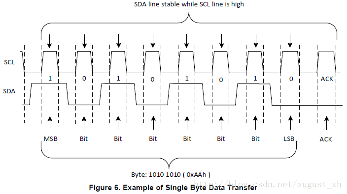
One data bit is transferred during each clock pulse of the SCL. One byte is comprised of eight bits on the SDA line. A byte may eighter be a device address, register address, or data written to or read from a slave. Data is transferred Most Significant Bit (MSB) first. Any number of data bytes can be transferred from the master to slave between the START and STOP conditions. Data on the SDA line must remain stable during the high phase of the clock period, as changes in the data line when the SCL is high are interpreted as control commands (START or STOP).
2.3 Acknowledge (ACK) and Not Acknowledge (NACK)
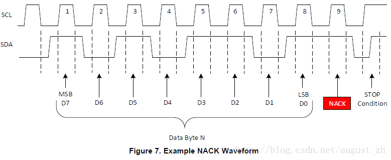
Each byte of data (including the address byte) is followed by one ACK bit from the receiver. The ACK bit allows the receiver to communicate to the transmitter that the byte was successfully received and another byte may be sent.
Before the receiver can send an ACK, the transmitter must release the SDA line. To send an ACK bit, the receiver shall pull down the SDA line during the low phase of the ACK/NACK-related clock period (period 9), so that the SDA line is stable low during the high phase of the ACK/NACK-related clock period. Setup and hold times must be taken into account.
When the SDA line remains high during ACK/NACK-related clock period, this is interpreted as a NACK. There are several conditions that lead to the generation of a NACK:
1. The receiver is unable to receive or transmit because it is performing some real-time function and is not ready to start communication with the master.
2. During the transfer, the receiver gets data or commands that it does not understand.
3. During the transfer, the receiver can not receive any more data bytes.
4. A master-receiver is done reading data and indicates this to the slave through a NACK.
3 I2C Data
Data must be sent and received to or from the slave devices, but the way that this is accomplished is by reading or writing to or from registers in the slave device.
Registers are locations in the slave’s memory which contain information, whether it be the configuration information, or some sampled data to send back to the master. The master must write information into thsese registers in order to instruct the slave device to perform a task.
While it is common to have registers in I2C slaves, please note that not all slave devices will have registers. Some devices are simple and contain only 1 register, which may be written directly to by sending the register data immediately after the slave address, instead of adressing a register. An example of a single-register device would be an 8-bit I2C switch, which is controlled via I2C commands. Since it has 1 bit to enable or disable a channel, there is only 1 register needed, and the master merely writes the register data after the slave address, skipping the register number.
3.1 Writing to a Slave On The I2C Bus
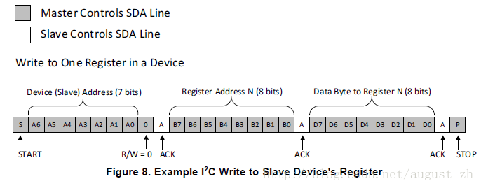
To write on the I2C bus, the master will send a start condition on the bus with the slave’s address, as well as the last bit (the R/W bit) set to 0, which signifies a write. After the slave sends the acknowledge bit, the master will then send the register address of the register it wishes to write to. The slave will acknowledge again, letting the master know it is ready. After this, the master will start sending the register data to the slave, until the master has sent all the data it needs to (sometimes this is only a single byte), and the master will terminate the transmission with a STOP condition. Figure 8 shows an example of wrting a single byte to a slave register.
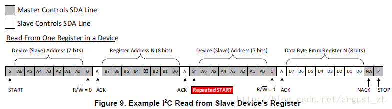
3.2 Reading From a Slave On The I2C Bus
Reading from a slave is very similar to writing, but with some extra steps. In order to read from a slave, the master must first instruct the slave which register it wishes to read from. This is done by the master starting off the transmission in a similar fashion as the write, by sending the adresses with the R/W bit equal to 0 (signifying a write), followed by the register address it wishes to read from. Once the slave acknowledges this register address, the master will send a START condition again, followed by the slave address with the R/W bit set to 1 (signifying a read). This time, the slave will acknowledge the read request, and the master releases the SDA bus, but will continue supplying the clock to the slave. During this part of transaction, the master will become the master-receiver, and the slave will become the slave-transmitter.
The master will continue sending out the clock pulses, but release the SDA line, so that the slave can transmit data. At the end of every byte of data, the master has received the number of bytes it is expecting, it will send a NACK, signaling to the slave to halt communications and release the bus. The master will follow this up with a STOP condition. Figure 9 shows an example of reading a single byte from a slave register.


 900
900


 被折叠的 条评论
为什么被折叠?
被折叠的 条评论
为什么被折叠?
 到【灌水乐园】发言


