


 ULINKplus 提供了一个隔离的 JTAG/SWD 接口,支持电压范围为 1.2V 到 5.5V,最大时钟速度可达 10MHz,且具有 1kV 的隔离等级。该接口允许热插拔到运行的目标。JTAG 和 Serial Wire 信号共享引脚,SWO 信号可选用于数据追踪。在 SWD 模式下,仅使用两个引脚进行通信,第三个引脚用于追踪数据。此外,ULINKplus 还包括一个适用于 STM32 开发板的 6 引脚 SWD 适配器。
JTAG/SWD Interface
The ULINKplus supports an isolated JTAG/SWD interface using a low-cost 10-pin (0.05") connector.
Technical characteristics
| Interface | Description |
|---|---|
| JTAG/SWD | Voltage range: 1.2 V .. 5.5 V Clock speed: configurable up to 10 MHz SWO trace capturing: data rate up to 50 Mbit/s (UART/NRZ Mode) Isolation: 1 kV Supports hot-plugging to a running target |
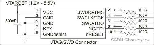
Interface Schematic
The target interface schematic shows the JTAG and Serial Wire interface circuits of ULINKplus. All pins are 1kV isolated and support hot-plugging while the target is running.
Use this schematic to help with board design, and for analyzing and debugging your target hardware.
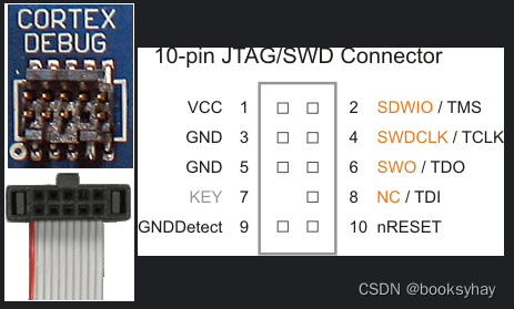
JTAG/SWD Connector
The 10-pin, 0.05" JTAG/SWD connector offers ITM and DWT trace information. In SWD mode, two pins are used for debugging: one bi-directional pin (SWDIO) transfers the information and the second pin (SWDCLK) clocks the data. A third pin (SWO) delivers the trace data at minimum system cost. The Serial Wire and JTAG pins are shared.
Note:
- KEY (position 7) has no pin and serves only as a key to properly orient the connector.
- VCC (pin 1) provides the supply voltage for the JTAG/SWD I/O driver and is required as ULINKplus has isolated connection.
- The 10-pin connector is a Samtec 10-pin: FTSH-105-01-L-DV-007-K connector with pin 7 removed. It's dimensions are: 0.25" x 0.188" (6.35mm x 4.78mm).
JTAG and Serial Wire Signals
Because the 10-pin JTAG/SWD connector supports both JTAG and Serial Wire signals, you can configure the debugger for either JTAG or Serial Wire mode to suit your Cortex device.
JTAG Signals
| Signal | Connects to... |
|---|---|
| TMS | Test Mode State pin -- Use 100K Ohm pull-up resistor to VCC. |
| TDO | Test Data Out pin. |
| TDI | Test Data In pin -- Use 100K Ohm pull-up resistor to VCC. |
| TCLK | Test CLocK pin -- Use 100K Ohm pull-down resistor to GND. |
| VCC | Positive Supply Voltage -- Power supply for JTAG interface drivers. |
| GND | Digital ground. |
| RESET | RSTIN/ pin -- Connect this pin to the (active low) reset input of the target CPU. |
Serial Wire Signals
The Serial Wire mode differs to JTAG debugging, because only two pins are used for the communication. A third pin can be used optionally to trace data. JTAG pins and SW pins are shared.
- TCLK is SWCLK (Serial Wire Clock)
- TMS is SWDIO (Serial Wire debug Data Input/Output)
- TDO is SWO (Serial Wire trace Output)
| Signal | Connects to... |
|---|---|
| SWDIO | Data I/O pin -- Use 100K Ohm pull-up resistor to VCC. |
| SWO | Optional trace output pin. |
| SWCLK | Clock pin -- Use 100K Ohm pull-down resistor to GND. |
| VCC | Positive Supply Voltage -- Power supply for JTAG interface drivers. |
| GND | Digital ground. |
| RESET | RSTIN/ pin -- Connect this pin to the (active low) reset input of the target CPU. |
Note:
- Usually, devices do not include pull-up or pull-down resistors on JTAG nor SW pins. Resistors should be added externally onto the board. However, do not add resistors when the device includes them already.
ULINK SWD Adapter
Many STM32 development boards do not have standard -pin Cortex Debug Connector. For such cases, the ULINKplus kit also includes an adapter for the 6-pin SWD interface which is frequently present on STM32 development boards. The figure below shows the adapter.
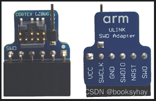
Pinout
The table below explains the SWD adapter pins in details. The Cortex debug connector is explained in the JTAG/SWD interface
| Signal | Description |
|---|---|
| VCC | Positive Supply Voltage -- Power supply for JTAG interface drivers. |
| SWCLK | Clock pin |
| GND | Digital ground. |
| SWDIO | Data I/O pin. |
| NRST | Reset input -- Connect this pin to the (active low) reset input of the target CPU. |
| SWO | Optional trace output pin. |
参考资料:


 1万+
1万+

 被折叠的 条评论
为什么被折叠?
被折叠的 条评论
为什么被折叠?
 到【灌水乐园】发言


