


前言:
续上章节UART后,此章讲解的IIC也是最常见的串行通讯,广泛应用于单片机和单片机之间通讯。同样这里IIC的具体原理讲解就不做介绍,不清楚的朋友可移步up主的个人专栏 ---- “串行通讯原理”中的“串行通讯 -- IIC通讯原理”,此专栏会有针对IIC的工作原理的详细介绍。
RIIC 寄存器基地址
| Base Address Name | Base Address |
| <RIIC0_base> | FFCA 0000H |
RIIC 时钟源选择
| Unit Name | Unit Clock Name | Supply Clock Name | Description |
| RIIC0 | PCLK | CKSCLK_IIIC | 通讯时钟 |
| 寄存器访问时钟 | CPUCLK2 | 总线时钟 | |
| 寄存器访问时钟 | CKSCLK_IIIC | 总线时钟 |
RIIC 接口框图

1.1、RIICnCR1 — IIC总线控制寄存器1
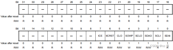
| Bit position | Bit Name | Function |
| 7 | ICE | I2C总线接口启用 0:禁用(RIICnSCL和RIICnSDA引脚未被驱动)。 1:使能(驱动RIICnSCL和RIICnSDA引脚)。 (该位选择RIIC复位或与IICRST相结合的内部复位 位)。 |
| 6 | IICRST | I2C总线接口内部复位 0:清除RIIC复位或内部复位。 1:表示发起RIIC复位或内部复位。 (清除位计数器和SCL/SDA输出锁存) |
| 5 | CLO | 拓展SCL时钟周期输出 0:不输出拓展SCL时钟周期(默认)。 1:输出拓展SCL时钟周期。 (CLO位在一个时钟周期输出后自动清除。) |
| 4 | SOWP | SCLO /SDAO写保护 0:可写位SCLO和SDAO。 1:保护位SCLO和SDAO。 (此位读为1。) |
| 3 | SCLO | SCL输出控制/监视器 ·读: 0: RIIC驱动RIICnSCL引脚低。 1: RIIC释放了RIICnSCL引脚。 ·写: 0: RIIC驱动RIICnSCL引脚低。 1: RIIC释放RIICnSCL引脚。 |
| 2 | SDAO | SDA输出控制/监视器 ·读: 0: RIIC驱动RIICnSDA引脚低。 1: RIIC释放RIICnSDA引脚。 ·写: 0: RIIC驱动RIICnSDA引脚低。 1: RIIC释放RIICnSDA引脚。 |
| 1 | SCL1 | SCL线路监测器 0: RIICnSCL线路低。 1: RIICnSCL线路高 |
| 0 | SDA1 | SDA线路监测器 0: RIICnSDA线路低。 1: RIICnSDA线路高。 |
1.2、RIICnSER — IIC总线状态使能寄存器

| Bit position | Bit Name | Function |
| 5 | DIDE | 设备id地址检测功能 0:关闭设备id地址检测功能。 1:启用设备id地址检测。 |
| 3 | GCE | 通用呼叫地址启用 0:关闭普通呼叫地址检测。 1:开启普通呼叫地址检测。 |
| 2 | SAR2 | 从地址寄存器2启用 0:禁用RIICnSAR2从地址。 1:使能RIICnSAR2从地址。 |
| 1 | SAR1 | 从地址寄存器1启用 0:禁用RIICnSAR1从地址。 1:使能RIICnSAR1从地址。 |
| 0 | SAR0 | 从地址寄存器0启用 0:禁用RIICnSAR0从地址。 1:使能RIICnSAR0从地址。 |
1.3、RIICnMR1 — IIC总线模式寄存器1
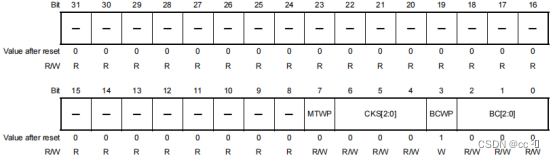
| Bit position | Bit Name | Function |
| 7 | MTWP | MST/TRS写保护 0:禁止写入RIICnCR2。MST和TRS位。 1:允许写入RIICnCR2。MST和TRS位。 |
| 6 - 4 | CKS | 内部参考时钟选择(IIC) B6 ~ B4 0 0 0: PCLK/1时钟 0 0 1: PCLK/2时钟 0 1 0: PCLK/4时钟 0 1 1: PCLK/8时钟 1 0 0: PCLK/16时钟 1 0 1: PCLK/32时钟 1 1 0: PCLK/64时钟 1 1 1: PCLK/128时钟 |
| 3 | BCWP | BC写保护 0:允许用BC[2:0]位写入值。(此位读为1) 1:保护BC[2:0]位。 |
| 2 - 0 | BC | 位计数器 B2 ~ B0 0 0 0: 9位 0 0 1: 2位 0 1 0: 3位 0 1 1: 4位 1 0 0: 5位 1 0 1: 6位 1 1 0: 7位 1 1 1: 8位 |
1.4、RIICnBRH — IIC总线波特率高位寄存器
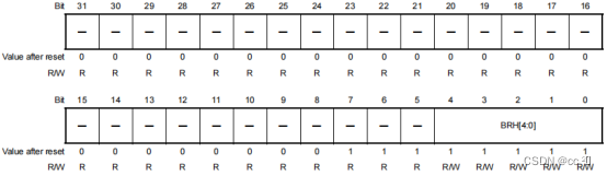
| Bit position | Bit Name | Function |
| 4 - 0 | BRH | 波特率周期的高位 SCL时钟周期的高位 |
1.5、RIICnBRL — IIC总线波特率低位寄存器
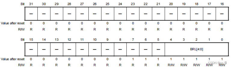
| Bit position | Bit Name | Function |
| 4 - 0 | BRL | 波特率周期的低位 SCL时钟周期的低位 |
1.6、RIICnMR2 — IIC总线模式寄存器2
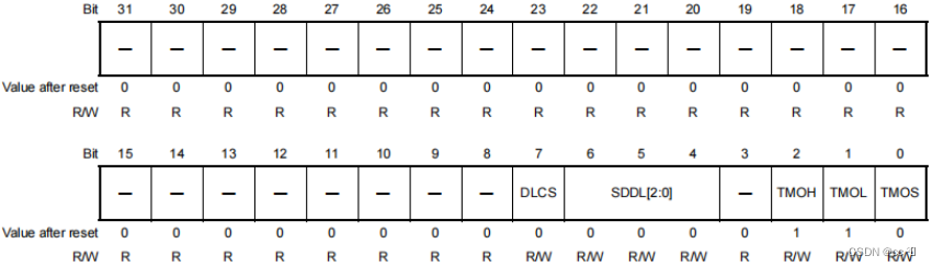
| Bit position | Bit Name | Function |
| 7 | DLCS | SDA输出延迟时钟源选择 0:选择内部参考时钟(IIC)作为时钟源SDA输出延迟计数器。 1:选择内部参考时钟(IIC/2)除以2作为时钟SDA输出延迟计数器。 |
| 6 - 4 | SDDL | SDA输出延迟时钟源选择SDA输出延迟计数器 当RIICnMR2.DLCS = 0 (iic) 时 B6 ~ B4 0 0 0:无输出延时 0 0 1: 1 IICf周期 0 1 0: 2 IICf周期 0 1 1: 3 IICf周期 1 0 0: 4 IICf周期 1 0 1: 5 IICf周期 1 1 0: 6 IICf周期 1 1 1: 7 IICf周期 当RIICnMR2.DLCS = 1 (iic/2) 时 B6 ~ B4 0 0 0:无输出延时 0 0 1: 1或2个IIC周期 0 1 0: 3或4个IIC周期 0 1 1: 5或6个IIC周期 1 0 0: 7或8个IIC周期 1 0 1: 9或10个IIC周期 1 1 0: 11或12个IIC周期 1 1 1: 13或14个IIC周期 0:选择内部参考时钟(IIC)作为时钟源 SDA输出延迟计数器。 1:选择内部参考时钟(IIC/2)除以2作为时钟SDA输出延迟计数器。 |
| 2 | TMOH | 超时H计数控制 0:当SCL线处于高电平时禁用计数。 1:当SCL线处于高电平时启用计数。 |
| 1 | TMOL | 超时L计数控制 0:当SCL线处于低电平时禁用计数。 1:在SCL线处于低电平时开启计数。 |
| 0 | TMOS | 超时检测时间选择 0:选择长模式。 1:选择短模式。 |
1.7、RIICnMR3 — IIC总线模式寄存器3
| Bit position | Bit Name | Function |
| 6 | WAIT | 是否等待: 0:不等待 (第九个时钟周期和第一个时钟周期之间的周期高电平。) 1:等待 (第9个时钟周期和第1个时钟周期之间的周期低电平。) |
| 5 | RDRFS | RDRF标志设置计时选择 0: RDRF标志设置在第九个SCL时钟周期的上升边缘。 (SCL线在第八个时钟周期的下降边缘处高电平。) 1: RDRF标志设置在第八个时钟周期的上升边缘。 (SCL线在第八个时钟周期的下降边缘保持低电平。) |
| 4 | ACKWP | 写保护 0:禁用修改ACKBT位。 1:表示启用修改ACKBT位。 |
| 3 | ACKBT | 传输确认 0:发送0作为确认位(ACK传输)。 1:发送a1作为确认位(NACK传输)。 |
| 2 | ACKBR | 接收确认 0:接收0作为确认位(ACK接收)。 1:接收a1作为确认位(NACK接收)。 |
| 1 - 0 | NF | 数字噪声滤波器级选择 B1 - B0 0 0:过滤掉最多一个IIC循环的噪声(1级滤波器)。 0 1:过滤掉最多两个IIC循环的噪声(2级滤波器)。 1 0:过滤掉最多三个IIC循环的噪声(3级滤波器)。 1 1:过滤掉最多4个IIC循环的噪声(4级滤波器)。 |
1.9、RIICnIER — IIC总线中断使能寄存器
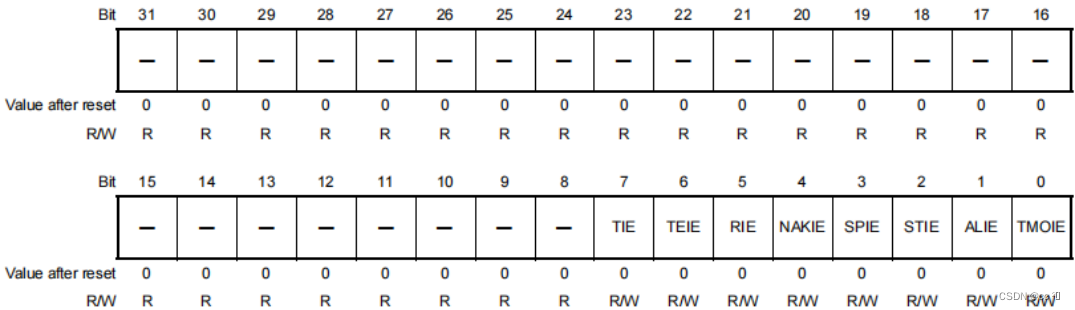
| Bit position | Bit Name | Function |
| 7 | TIE | 传输数据空中断启用 0:禁用发送数据空中断请求(INTRIICnTI)。 1:使能发送数据空中断请求(INTRIICnTI)。 |
| 6 | TEIE | 发送结束中断启用 0:禁用发送端中断请求(INTRIICnTEI)。 1:使能发送端中断请求(INTRIICnTEI)。 |
| 5 | RIE | 接收完全中断启用 0:禁用接收完整中断请求(INTRIICnRI)。 1:使能接收完整中断请求(INTRIICnRI)。 |
| 4 | NAKIE | 启用NACK接收中断 0:关闭NAKI (NACK receive interrupt request)功能。 1:启用NAKI (NACK receive interrupt request)功能。 |
| 3 | SPIE | 停止条件检测中断启用 0:禁用停止条件检测中断请求。 1:使能停止条件检测中断请求。 |
| 2 | STIE | 启动条件检测中断启用 0:关闭启动条件检测中断请求。 1:启用启动条件检测中断请求。 |
| 1 | ALIE | 仲裁丢失中断启用 0:关闭ALI(仲裁丢失中断请求)功能。 1:启用ALI (仲裁丢失中断请求)功能。 |
| 0 | TMOIE | 启用超时中断 0:关闭TMOI (超时中断请求)功能。 1:开启TMOI (超时中断请求)功能。 |
例程:
/*****************************************************************************
* Function Name : void R_IIC_Init( void )
* Description : This function initialize IIC.
* Argument : none
* Return Value : none
******************************************************************************/
void R_IIC_Init( void )
{
uint32_t reg32_value;
/* Set the interrupt flags */
INTC2MKRIIC0TI = 1U;
INTC2RFRIIC0TI = 0U;
INTC2TBRIIC0TI = 1U;
INTC2MKRIIC0TEI = 1U;
INTC2RFRIIC0TEI = 0U;
INTC2TBRIIC0TEI = 1U;
INTC2MKRIIC0RI = 1U;
INTC2RFRIIC0RI = 0U;
INTC2TBRIIC0RI = 1U;
INTC2MKRIIC0EE = 1U;
INTC2RFRIIC0EE = 0U;
INTC2TBRIIC0EE = 1U;
/* Disabled I2C Bus Interface
RIICnCR1 - I2C Bus Control Register 1
b31:b 8 - Reserved set to 0
b 7 ICE - I2C Bus Interface Enable - Disabled (the RIICnSCL and RIICnSDA pins are not driven). set to 0
b 6 IICRST - I2C Bus Interface Internal Reset - not change.
b 5 CLO - Extra SCL Clock Cycle Output - not change.
b 4 SOWP - SCLO/SDAO Write Protect - not change.
b 3 SCLO - SCL Output Control/Monitor - not change.
b 2 SDAO - SDA Output Control/Monitor - not change.
b 1 SCLI - SCL Line Monitor - not change.
b 0 SDAI - SDA Line Monitor - not change. */
RIIC0CR1 &= 0xFFFFFF7FUL;
/* I2C Bus Interface Internal Reset
RIICnCR1 - I2C Bus Control Register 1
b31:b 8 - Reserved set to 0
b 7 ICE - I2C Bus Interface Enable - not change.
b 6 IICRST - I2C Bus Interface Internal Reset - Initiates the RIIC reset or internal reset. set to 1
b 5 CLO - Extra SCL Clock Cycle Output - not change.
b 4 SOWP - SCLO/SDAO Write Protect - not change.
b 3 SCLO - SCL Output Control/Monitor - not change.
b 2 SDAO - SDA Output Control/Monitor - not change.
b 1 SCLI - SCL Line Monitor - not change.
b 0 SDAI - SDA Line Monitor - not change. */
RIIC0CR1 |= 0x00000040UL;
/* Enabled I2C Bus Interface
RIICnCR1 - I2C Bus Control Register 1
b31:b 8 - Reserved set to 0
b 7 ICE - I2C Bus Interface Enable - Enabled (the RIICnSCL and RIICnSDA pins driven). set to 1
b 6 IICRST - I2C Bus Interface Internal Reset - not change.
b 5 CLO - Extra SCL Clock Cycle Output - not change.
b 4 SOWP - SCLO/SDAO Write Protect - not change.
b 3 SCLO - SCL Output Control/Monitor - not change.
b 2 SDAO - SDA Output Control/Monitor - not change.
b 1 SCLI - SCL Line Monitor - not change.
b 0 SDAI - SDA Line Monitor - not change. */
RIIC0CR1 |= 0x00000080UL;
/* Slave address in RIICnSAR0 is enabled.
RIICnSER - I2C Bus Status Enable Register
b31:b 6 - Reserved set to 0
b 5 DIDE - Extra SCL Clock Cycle Output - Device-ID address detection is disabled. set to 0
b 4 - Reserved set to 0
b 3 GCE - SCL Output Control/Monitor - General call address detection is disabled. set to 0
b 2 SAR2 - SDA Output Control/Monitor - Slave address in RIICnSAR2 is disabled. set to 0
b 1 SAR1 - SCL Line Monitor - Slave address in RIICnSAR1 is disabled. set to 0
b 0 SAR0 - SDA Line Monitor - Slave address in RIICnSAR0 is enabled. set to 1 */
RIIC0SER = 0x00000001UL;
/* Internal Reference Clock Selection.
RIICnMR1 - I2C Bus Mode Register 1
b31:b 8 - Reserved set to 0
b 7 MTWP - MST/TRS Write Protect - not change.
b 6:b 4 CKS - Internal Reference Clock Selection - PCLK/16 clock. set to 100'b
b 3 BCWP - BC Write Protect - not change.
b 2:b 0 BC - Bit Counter - not change. */
RIIC0MR1 |= 0x00000030UL; /* 40MHz / 8 */
RIIC0BRH = 0xF6U; /* 100kbps */
RIIC0BRL = 0xF9U;
/* Set the I2C Bus Mode.
RIICnMR2 - I2C Bus Mode Register 2
b31:b 8 - Reserved set to 0
b 7 DLCS - SDA Output Delay Clock Source Selection - not change.
b 6:b 4 SDDL - SDA Output Delay Counter - not change.
b 3 - Reserved set to 0
b 2 TMOH - Timeout H Count Control - not change.
b 1 TMOL - Timeout L Count Control - not change.
b 0 TMOS - Timeout Detection Time Selection - not change. */
RIIC0MR2 = 0x00000006UL;
/* Set the I2C Bus Mode.
RIICnMR3 - I2C Bus Mode Register 3
b31:b 7 - Reserved set to 0
b 6 WAIT - WAIT - No WAIT. set to 0
b 5 RDRFS - RDRF Flag Set Timing Selection - The RDRF flag is set at the rising edge of the
ninth SCL clock cycle. set to 0
b 4 ACKWP - ACKBT Write Protect - Modification of the ACKBT bit is enabled. set to 1
b 3 ACKBT - Transmit Acknowledge - A 0 is sent as the acknowledge bit. set to 0
b 2 ACKBR - Receive Acknowledge - A 0 is received as the acknowledge bit. set to 0
b 1:b 0 NF - Digital noise Filter Stage Selection - Noise of up to one IIC cycle is filtered out. set to 00'b */
RIIC0MR3 = 0x00000010UL;
/* Set the I2C Bus functions.
RIICnFER - I2C Bus Function Enable Register
b31:b 7 - Reserved set to 0
b 6 SCLE - SCL Synchronous Circuit Enable - An SCL synchronous circuit is unused. set to 0
b 5 NFE - Digital Noise Filter Circuit Enable - A digital noise filter circuit is unused. set to 0
b 4 NACKE - NACK Reception Transfer Suspension Enable - Transfer operation is suspended during NACK reception. set to 1
b 3 SALE - Slave Arbitration-Lost Detection Enable - Slave arbitration-lost detection is disabled. set to 0
b 2 NALE - NACK Transmission Arbitration-Lost
Detection Enable - NACK transmission arbitration-lost detection is disabled. set to 0
b 1 MALE - Master Arbitration-Lost Detection Enable - Master arbitration-lost detection is disabled. set to 0
b 0 TMOE - Timeout Function Enable - The timeout function is disabled. set to 0 */
RIIC0FER = 0x00000010UL;
/* Set the Interrupts.
RIICnIER - I2C Bus Interrupt Enable Register
b31:b 8 - Reserved set to 0
b 7 TIE - Transmit Data Empty Interrupt Enable - Transmit data empty interrupt request (INTIICnTI) is enabled. set to 1
b 6 TEIE - Transmit End Interrupt Enable - Transmit end interrupt request (INTIICnTEI) is enabled. set to 1
b 5 RIE - Receive Complete Interrupt Enable - Receive complete interrupt request (INTIICnRI) is enabled. set to 1
b 4 NAKIE - NACK Reception Interrupt Enable - NACK reception interrupt request (NAKI) is disabled. set to 0
b 3 SPIE - Stop Condition Detection Interrupt Enable - Stop condition detection interrupt request (SPI) is enabled. set to 1
b 2 STIE - Start Condition Detection Interrupt Enable - Start condition detection interrupt request (STI) is disabled. set to 0
b 1 ALIE - Arbitration-Lost Interrupt Enabl e - Arbitration-lost interrupt request (ALI) is disabled. set to 0
b 0 TMOIE - Timeout Interrupt Enable - Timeout interrupt request (TMOI) is disabled. set to 0 */
RIIC0IER = 0x000000E8UL;
/* Alternative function port settings */
/* RIIC0SDA(P0_11:CN1D-14pin) 1'nd Alternative (output/input) */
/* RIIC0SCL(P0_12:CN1D-15pin) 1'nd Alternative (output) */
#if 1
reg32_value = PORTPODC0 | 0x00001800UL;
do
{
PORTPPCMD0 = 0xA5U;
PORTPODC0 = reg32_value;
PORTPODC0 = (uint32_t)(~reg32_value);
PORTPODC0 = reg32_value;
} while ( PORTPPROTS0 != 0x00000000UL );
#endif
PORTPIPC0 &= 0xE7FFU; // must be 0
PORTPBDC0 |= 0x1800U; // open chain
//PBDC0 &= 0xE7FFU; // open chain
PORTPFCAE0 &= 0xE7FFU; // mode 1
PORTPFCE0 &= 0xE7FFU; // mode 1
PORTPFC0 &= 0xE7FFU; // mode 1
PORTPMC0 |= 0x1800U; // alternative mode
PORTPM0 &= 0xE7FFU; // output
/* I2C Bus Interface Internal Reset
RIICnCR1 - I2C Bus Control Register 1
b31:b 8 - Reserved set to 0
b 7 ICE - I2C Bus Interface Enable - not change.
b 6 IICRST - I2C Bus Interface Internal Reset - Clears the RIIC reset or internal reset. set to 0
b 5 CLO - Extra SCL Clock Cycle Output - not change.
b 4 SOWP - SCLO/SDAO Write Protect - not change.
b 3 SCLO - SCL Output Control/Monitor - not change.
b 2 SDAO - SDA Output Control/Monitor - not change.
b 1 SCLI - SCL Line Monitor - not change.
b 0 SDAI - SDA Line Monitor - not change. */
RIIC0CR1 &= 0xFFFFFFBFUL;
/* interrupt mask release */
INTC2MKRIIC0TI = 0U;
INTC2MKRIIC0TEI = 0U;
INTC2MKRIIC0RI = 0U;
INTC2MKRIIC0EE = 0U;
}


 255
255


 被折叠的 条评论
为什么被折叠?
被折叠的 条评论
为什么被折叠?
 到【灌水乐园】发言


