


调试接口框图
ARM-M0《ARM Cortex-M0.pdf》手册上提到的调试框图如下:

《debug_interface_v6_0_architecture_specification_IHI0074A.pd》提到的调试框图如下:

由此可知DAP中分为了AP和DP
再看m3内核框图:
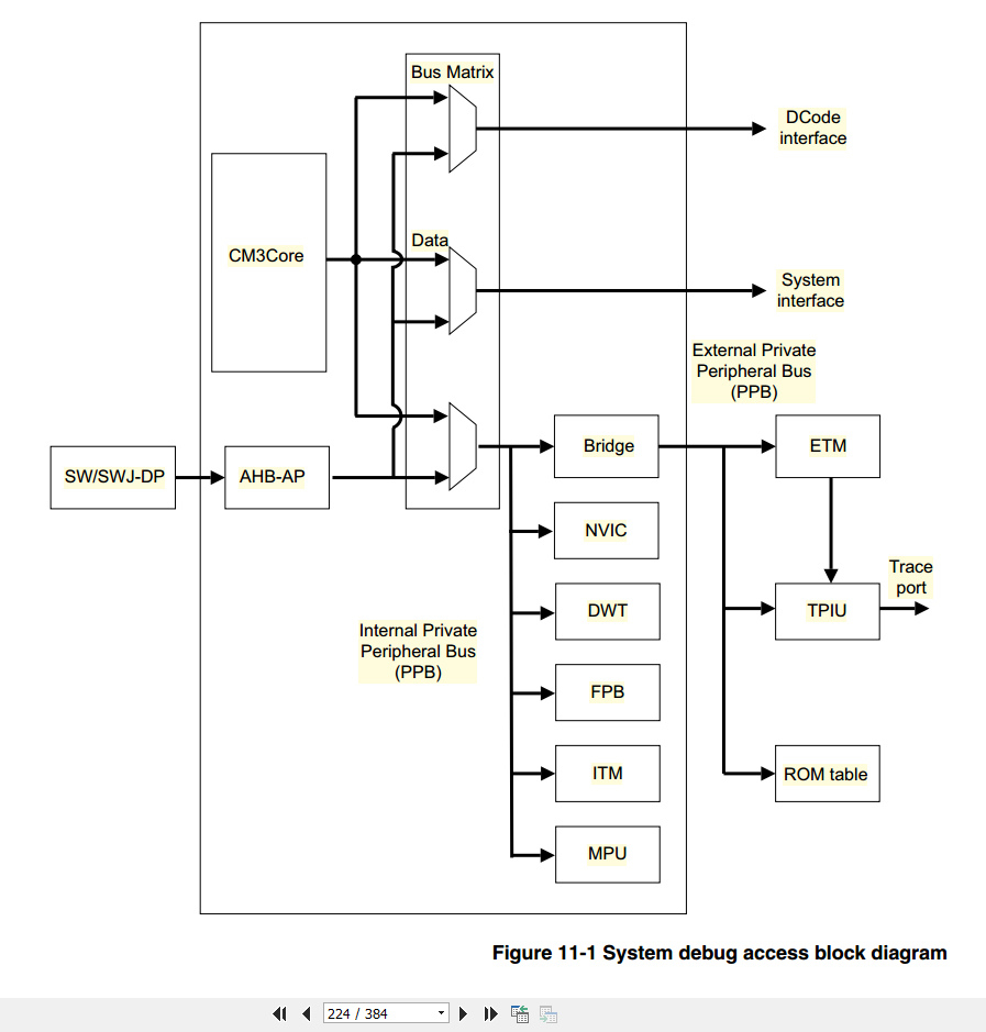
从这里可以看到AP是在芯片中的,而SWDP是在外面的(SWD仿真器)。
SWD时序


关于一些中国网友的解释请看:https://blog.csdn.net/baiyibin0530/article/details/51682179
内容摘录如下:
以下我的模拟SWD接口的板子简称为Host,目标MCU(即我要连接的板子)简称为Target。
SWD协议
故名思议,串行总线调试接口。我们需要3根线与目标MCU相连,SWDIO,SWDCLK和GND。
-SWDIO 为双向Data口,主机到目标的数据传送。
-SWDCLK 为时钟口,主机驱动。
-GND GND脚。
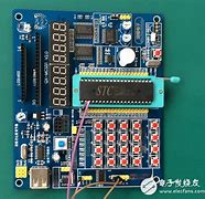
首先参考《ARM Debug Interface V5》(注:该文档已有更新版本,并且对V5版本做了勘误),对一些相关的协议相关说明有了较浅的认识。那接下来便找了个带SWD接口的板子,我这首先选了STM32F030,因为以后可以为生产线做离线编程器,当然随后也出现了一些问题,下文会说明。
连上相关物理连线,开始折腾。
看手册中有几个相对较重要的时序说明。
Trn-Trn:即Line turn-round,当总线上的数据传输方向发送改变时(比如由Host->Target变为Target->Host),需要插入Trn,Trn为一个CLK时序,关于对于Trn的理解自己也有些疑问。
Idle cycles:在一个总线完成后,可以立即进入下一个总线操作或者是勒令总线进入Idle 状态,此时可以插入Idle cycle。在这我用连续送出8个’0b0’来使得总线进入Idle状态。
Parity :校验位,这个比较简单。分两个内容对命令头进行校验和对数据进行校验。命令头下文会说明。数据校验是对Data的0b0-0b31进行校验,如果‘1’的个数为奇数那校验位就为‘0b1’,如果‘0b1’的个数为偶数校验位就为‘0b0’。
理解了这几个,我们接下来看读写命令。
每个读写命令之前都会有个Host->Target的数据头。每个数据头为1Byte.
-Start 起始位,始终为1,这也是Target判断总线从空闲状态退出的条件。
-APnDP 选择要访问的是DP寄存器还是AP寄存器。
- Rnw 选择是读还是写。
-A[2:3] DP或者AP寄存器的地址,注意它是低位在前。比如寄存器DP寄存器 Select 它的地址为0x08,那这儿的A为C(0b1000),显然A[2:3]就为01。
-Praity 校验位,它是APnDP、RnW和A[2:3]共4个bit的校验位。
-Stop 停止位。始终为0。
-Park 该位确切来说应该始终为1,ADI V5中描述此位由总线上拉,但由于总线的上拉能力不足,会导致Target识别不了这个1。该勘误在ADI V5.2中有说明。
读命令为数据头+Trn+ACK+RDATA+Parity构成,但实际操作发现Trn这位是忽略掉的(所以不知道对此Trn的理解是否有误),及发送完数据头后立即读入ACK,判断Target是否正确响应。
写命令为数据头+Trn+ACK+Trn+WDATA+Parity,在这不同的是,在写命令时必须要考虑2个Trn的位置。
看协议中首先在连接Target时需要进行LineReset,这个是最基础也是最最简单的命令。
具体实现为首先保证Host连续送出至少50个“1”,使得Target进行Line Reset,至少插入2个Idle,然后可以读取目标板的IDR,判断Target的类型。
理解了整个,然后就进行操作验证,发现偶尔可以有数据ACK,继续查看手册,发现需要进行JTAG和SWD的切换操作。查看手册发现切换操作的时序如下。
可以简化为先进行一次LineReset,随后发送0X79,0XE7(高字节首先传送),接着再一次LineReset,随后便可以读IDR。但是发现了问题,用此方式可以读取到STM32F103的IDR,但STM32F030不行,在ARM网站查阅相关资料,发现了这个。
上图主要说在一个更早的协议中需要发送如下命令才能进行JTAG和SWD的切换。就是要发送0X6D,0XB7,尝试了下,这下能顺利读取到IDR了。疑惑的是STM32F0系列比F1出来要晚,居然用的老版本的协议?
既然能够获取到IDR了,那接下来可以尝试着进行连接到AHB-AP了。用DP寄存器的SELECT来进行选择。这儿为了能够使得结果明显和确切,我选择了读取AP 0XFC 的IDR寄存器,来获取AP的特性,因为这个数据是只读的和确切的。
首先要用写入DP寄存器SELECT。
SELECT的具体描述可以参见ADI V5手册,在这有个说明,当时走了弯路。SELECT寄存器中有个APSEL选择位,这个是选择当前连接的AP,手册中没有详细说明它的定义。后来在另外的文档中发现该值为0x00,AHB-AP。APBANKSEL为选择需要访问的BANK地址,比如IDR寄存器的地址为0XFC,那它的BANKSEL为F,如果为TAR寄存器,那它的BANKSEL为0。
连接到AHB-AP后就能进行你想要的操作了。比如我可以读取MCU的独立ID,就可以通过MEM-AP来操作。也可以对MCU进行擦除或者编程。
在做编程之前,首先将MCU进入Halt状态,然后访问MCU相关FLASH控制寄存器进行读写即可。
在STM32F030编程时需要注意的是STM32F030的FLASH的传输方式,我未采用Packet的传输方式。
LineReset代码
static void SwdLineReset(void)
{
u8 i;
SWD_OUT;
SWD_DIO_H;
for(i=0;i<56;i++)
{
SWD_Delay();
SWD_CLK_H;
SWD_Delay();
SWD_CLK_L;
}
}
写命令头函数
static void SwdSendByte(u8 dat)
{
u8 i;
SWD_OUT;
for(i=0;i<8;i++)
{
if((dat&0x80)==0x80)
{
SWD_DIO_H;
}
else
{
SWD_DIO_L;
}
dat<<=1;
SWD_CLK_H;
SWD_Delay();
SWD_CLK_L;
SWD_Delay();
}
}
读取一个data函数
static u32 SeqRead(u8 cmd)
{
u32 dat=0;
u8 i=0;
SwdSendByte(cmd);
SWD_IN;
for(i=0;i<3;i++)//ack 此处需要处理判断
{
SWD_CLK_H;
SWD_Delay();
SWD_CLK_L;
SWD_Delay();
}
dat=0;
for(i=0;i<32;i++)
{
dat=dat>>1;
SWD_CLK_H;
SWD_Delay();
SWD_CLK_L;
if(SWD_DII)
{
dat|=0x80000000;
}
SWD_Delay();
}
//parity
SWD_IN; //trn
for(i=0;i<2;i++)
{
SWD_CLK_H;
SWD_Delay();
SWD_CLK_L;
SWD_Delay();
}
SWD_DIO_L;
SWD_OUT;
for(i=0;i<5;i++)
{
SWD_CLK_H;
SWD_Delay();
SWD_CLK_L;
SWD_Delay();
SWD_CLK_H;
SWD_Delay();
SWD_CLK_L;
SWD_Delay();
}
SWD_IN; //trn
return dat;
}
SWD主机
这里分享一个SWD master的例子:https://github.com/MarkDing/swd_programing_sram
简介如下:
Programming internal SRAM over SWD
1. Introduction
This documentation describe how to programming ARM Cortex M3 internal SRAM over SWD(Serial Wire Debug) interface. For this purpose, something we too know.
- SWD communication protocol. We need to know Low level timing requirement, that is foundation to exchange command and data between debugger and target MCU.
- Read/write data from/to internal SRAM. We need to know how to program firmware into desired address, like SRAM(0x20000000). That needs us to know SW-DAP registers usage. Pass address and data over those registers and then into internal SRAM.
- Make code running from SRAM. We need to change vector table entry from internal flash to SRAM; And SP and PC also needed change to SRAM location. That need us to know the cortex M3 debug and system registers usage.
We choose Silabs SiM3U167 as target MCU in this implementation. We implement a high level protocol with python script, it calls Silabs provided DLL file interface to access Silabs USB Debug Adapter. Also, we provide a firmware running from C8051F380, it contains a full implementation on both low level communicating timing and high level programming SRAM protocol.
2. Serial Wire Debug overview
Serial Wire Debug (SWD) is a 2-pin (SWDIO/SWCLK) electrical alternative JTAG interface that has the same JTAG protocol on top. SWD uses an ARM CPU standard bi-directional wire protocol, defined in the ARM Debug Interface v5. This enables the debugger to become another AMBA bus master for access to system memory and peripheral or debug registers.
The Debug Access Port(DAP) is split into two main control units. the Debug Port (DP) and the Access Port (AP), and the physical connection to the debugger is part of the DP. The DAP supports two types of access, Debug Port (DP) accesses and Access Port (AP)accesses. External device to communicate directly with Serial Wire Debug Port(SW-DP) over SWDIO/SCLK pins. And SW-DP in turn can access one or several Access Ports(APs) the give access to the rest of the system. The MEM-AP is important AP which provide a way to access all memory and peripheral registers residing on the internal AHB/APB buses.
Figure 1 ARM Debug Interface MEM-AP Implementation
One of the four registers within the DP is the AP Select Register, SELECT. This register specifies a particular Access Port, and a bank of four 32-bit words within the register map of that AP. It enables up to 256 Access Ports to be implemented, and gives access to any one of 16 four-word banks of registers on the selected AP.
3. SWD protocol
This section gives an overview of the bi-directional operation of the protocol. It illustrates each of the possible sequences of operations on the Serial Wire Debug interface data connection.
3.1. Connection and line reset sequence
The SW-DP must use connection sequence of 50 clock cycles with data = 1. And this sequence is also used as a line reset sequence which requires 50 consecutive 1s on the data input.
JTAG to SWD switching
SWJ-DP enables either an SWD or JTAG protocol to be used on the debug port. To do this, it implements a watcher circuit that detects a specific 16-bit selection sequence on the SWDIOTMSpin:
The 16-bit JTAG-to-SWD select sequence is defined to be 0b0111100111100111, MSB first. This can be represented as 16'h79E7 if transmitted MSB first or 16'hE79E if transmitted LSB first.
The host must read IDCODE register after line request sequence. This requirement gives confirmation that correct packet frame alignment has been achieved.
3.2. Successful transaction operation
A successful transaction contains three phases.
- Host sending an eight-bit write packet request to target.
- Target response with a three-bit OK acknowledge to host.
- A 33-bit data phase, either from host or target depends on write/read operation.
Figure 2 Serial Wire Debug successful write operation
3.2.1. Packet request phase
The request phase consists of 8 bits. The meaning of each bit in the request is illustrated below.
Start-- A single start bit, with value 1.APnDP-- A single bit, indicating whether the Debug Port or the Access Port Access Register is to be accessed. 1 for accessing AP.RnW-- A single bit, this bit is 0 for an write access, or 1 for a read access.A[2:3]-- Two bits, giving the A[3:2] address field for the DP or AP register address.Parity-- A single odd parity bit is made over the APnDP, RnW and A[2:3] bits. The number of bits set to 1 is odd, then the parity bit is set to 1.Stop-- A single stop bit. In the synchronousSWD protocol this is always 0.Park-- A single bit, with value 1.
3.2.2. Acknowledge response phase
ACK phase is a three-bit(LSB-first) target to host response. Three type ACK response.
OK Response-- It indicates successful operation, value is b001.WAIT response-- The host must retry the operation later, value is b010.FAULT response-- If the target responds with FAULT, an error has occurred and one of the sticky bits in CTRL/STAT is set. The host can check the sticky error bits to see what kind of error has occurred. It must clear the sticky bits in ABORT register before using any AP commands, because the target will always respond with FAULT as long as one of the sticky error bits are set. Value is b100.
3.2.3. Data transfer phase
It contains 32 data bits and 1 parity bit. The The parity check is made over the 32 data bits. The number of bits set to 1 is odd, then the parity bit is set to 1.
3.2.4. Turnaround period
From figure above, there is Trn -- Turnaround period between each phase. Every time the SWDIO changes data direction, a one-cycle turnaround period is inserted which both sides should ignore. This means there is always a turnaround period between the request and acknowledge. On a write request, there is a turnaround period between acknowledge and the data phase. On a read request there is a a turnaround after the data phase.
4. Serial Write Debug Port(SW-DP) Registers
This section will give a brief overview over the SW-DP registers.
Table 1 SW-DP registers
| Address | Read | Write |
|---|---|---|
| 0x00 | IDCODE | ABORT |
| 0x04 | CTRL/STAT | CTRL/STAT |
| 0x08 | RESEND | SELECT |
| 0x0C | RDBUFF | N/A |
4.1. The Identification Code Register, IDCODE
IDCODE register provides a identification information about SW-DP. On the EFM32 or SiM3U devices with a Cortex-M3 or Cortex-M4 core this register should read 0x2BA01477. For devices with a CortexM0+ core the register should read 0x0BC11477.
4.2. The AP Abort Register, ABORT
ABORT register main purpose is to force a DAP abort, and on a SW-DP it is also used to clear error and sticky flag conditions. Here are the bit assignments of AP Abort register.
Table 2 ABORT register bit assignments
| Bits | Function | Description |
|---|---|---|
| [31:5] | - | Reserved |
| [4] | ORUNERRCLR | Write 1 to this bit to clear the STICKYORUN overrun error flag to 0. |
| [3] | WDERRCLR | Write 1 to this bit to clear the WDATAERR write data error flag to 0 |
| [2] | STKERRCLR | Write 1 to this bit to clear the STICKYERR sticky error flag to 0. |
| [1] | STKCMPCLRa | Write 1 to this bit to clear the STICKYCMP sticky compare flag to 0. |
| [0] | DAPABORT | Write 1 to this bit to generate a DAP abort. This aborts the current AP transaction. Do this only if the debugger has received WAIT responses over an extended period. |
You might want to find what caused the flag to be set to 1. Typically:
- For the
STICKYCMPorSTICKYERRflag, you must find which location was accessed to cause the flag to be set to 1. - For the
WDATAERRflag, you must resend the corrupted data. - For the
STICKYORUNflag, you must find which DP or AP transaction caused the overflow. You then have to repeat your transactions from that point.
4.3. The Control/Status Register, CTRL/STAT
CTRL/STAT register provides control of the DP and status information about the DP.
Figure 3 Control/Status Register bit assignments
- Bit [28]
CDBGPWRUPREQis the signal from the debug interface to the power controller, used to request the system power controller to fully power-up and enable clocks in the debug power domain. - Bit [30]
CSYSPWRUPREQis the signal from the debug interface to the power controller, used to request the system power controller to fully power-up and enable clocks in the system power domain.
The debugger must write a 1 to the CDBGPWRUPREQ and CSYSPWRUPREQ bits before using the AHB-AP. The STICKYERR bit is set if an error is returned by a AP transaction. While the STICKYERR bit is set any SWD request will return a FAULT response. To clear the STICKYERR bit, use the ABORT register.
4.4. The AP Select Register, SELECT
SELECT register specifies a particular Access Port, and a bank of four 32-bit words within the register map of that AP. It enables up to 256 Access Ports to be implemented, and gives access to any one of 16 four-word banks of registers on the selected AP.
Table 3 Bit assignments for the AP Select Register, SELECT
| Bits | Function | Description |
|---|---|---|
| [31:24] | APSEL | Selects the current AP. |
| [7:4] | APBANKSEL | Selects the active four-word register bank on the current AP |
4.5. The Read Buffer, RDBUFF
RDBUFF register return the result of a previous read, without initiating a new AP transaction.
If you require the value from an AP register read, that A read of the DP Read Buffer must be followed.
5. Memory Access Port(MEM-AP) Registers
A MEM-AP provides a DAP with access to a memory subsystem. Since memory, peripherals and debug components are all memory mapped, the MEM-AP can be used to both program and debug Cortex M3.
Table 4 MEM-AP registers
| Address | Bank | Function | Description |
|---|---|---|---|
| 0x00 | 0x00 | CSW | Control/Status Word Register |
| 0x04 | 0x00 | TAR | Transfer Address Register |
| 0x0C | 0x00 | DRW | Data Read/Write Register |
| 0xFC | 0x0F | IDR | Identification Register |
5.1. Control/Status Word (CSW) Register
CSW register configures and controls accesses through the MEM-AP to or from a connect memory system.
Table 5 Bit assignments for the MEM-AP Control/Status Word Register, CSW
| Bits | Function | Description |
|---|---|---|
| [30:24] | Prot | Bus access protection control. This field enables the debugger to specify protection flags for a debug access. |
| [5:4] | AddrInc | Address auto-increment and packing mode. |
| [2:0] | Size | b000: 8 bits; b001: 16 bits; b010: 32 bits |
5.2. The Transfer Address Register (TAR)
TAR register holds the memory address to be accessed. The contents of TAR can be incremented automatically on a successful DRW access with b01 set in AddrInc field of CSW register.
5.3. The Data Read/Write Register (DRW)
DRW register is used to either write or read from the address held in TAR. To write a value to an internal memory address, first write the address to the TAR register, then write the value to DRW. To read a memory address, first write the address to TAR, then read the value in DRW.
5.4. The Identification Register, (IDR)
IDR register identifies the Access Port. To read this register, the APBANKSEL field should be set to 0xF. And then IDR register can be read with address 0x0C(ADDR[3:2] = b11). The IDR register should return the value 0x24770011 on devices with a Cortex-M3 or Cortex-M4 core. On devices with a Cortex-M0+ it should return 0x0477003
6. Debug and system Registers
This section will go through the Cortex M3 Debug registers. With debug registers, we can set core into halt mode and can change core registers, like SP or PC.
Table 6 Debug and system registers
| Address | Name | Description |
|---|---|---|
| 0xE000EDF0 | DHCSR | Debug Halting Control and Status Register |
| 0xE000EDF4 | DCRSR | Debug Core Register Selector Register |
| 0xE000EDF8 | DCRDR | Debug Core Register Data Register |
| 0xE000EDFC | DEMCR | Debug Exception and Monitor Control Register |
| 0xE000ED0C | AIRCR | Application Interrupt and Reset Control Register |
6.1. Debug Halting Control and Status Register, DHCSR
DHCSR register controls halting debug. Halting debug is enabled when C_DEBUGEN is set to 1.
Table 7 DHCSR bit assignments
| Bits | Name | Function |
|---|---|---|
| [31:16] | DBGKEY | Debug key: A debugger must write 0xA05Fto this field to enable write accesses to bits [15:0], otherwise the processor ignores the write access. |
| [16] | S_REGRDY | A handshake flag for transfers through the DCRDR: 0 = There has been a write to the DCRDR, but the transfer is not complete; 1 = The transfer to or from the DCRDR is complete. |
| [0] | C_DEBUGEN | Halting debug enable bit: 1 = Enabled |
6.2. Debug Core Register Selector Register, DCRSR
DCRSR register provides debug access to the ARM core registers, special-purpose registers, and Floating-point extension registers. A write to DCRSR specifies the resister to transfer.
Table 8 DCRSR bit assignments
| Bits | Name | Function |
|---|---|---|
| [16] | REGWnR | 0 = read; 1= write |
| [6:0] | REGSEL | Specifies the ARM core register, special-purpose register, or Floating-point extension register, to transfer: R0-R12, SP, LR, DebugReturnAddr, xPSR, MSP, PSP, etc. |
DebugReturnAddress is the address of the first instruction to be executed on exit from Debug state.
6.3. Debug Core Register Data Register, DCRDR
DCRDR register provides debug access to ARM core register, special-purpose registers,and Floating-point extension registers. The DCRDR is the data register for these accesses.
Use of DCRSR and DCRDR
- To transfer a data word to an ARM core register, special-purpose register, orFloating-point extension register, a debugger:
- Writes the required word to DCRDR.
- Writes to the DCRSR, with the REGSEL value indicating the required register, and the REGWnR bit as 1 to indicate a write access. This write clears the DHCSR S_REGRDY bit to 0.
- If required, polls DHCSR until DHCSR.S_REGRDY reads-as-one. This shows that the processor has transferred the DCRDR value to the selected register.
- To transfer a data word from an ARM core register, special-purpose register, or Floating-point extension register, a debugger:
- Writes to the DCRSR, with the REGSEL value indicating the required register, and the REGWnR bit as 0 to indicate a read access. This write clears the DHCSR.S_REGRDY bit to 0.
- Polls DHCSR until DHCSR.S_REGRDY reads-as-one. This shows that the processor has transferred the value of the selected register to DCRDR.
- Reads the required value from DCRDR.
6.4. Debug Exception and Monitor Control Register, DEMCR
DEMCR register manages vector catch behavior and DebugMonitor handling when debugging. Bits [23:16] provide DebugMonitor exception control. Bits [15:0] provide Debug state, halting debug, control.
Table 9 DEMCR bit assignments
| Bits | Name | Function |
|---|---|---|
| [10] | VC_HARDERR | Enable halting debug trap on a HardFault exception |
| [9] | VC_INTERR | Enable halting debug trap on a fault occurring during exception entry or exception return. |
| [8] | VC_BUSERR | Enable halting debug trap on a BusFault exception. |
| [7] | VC_STATERR | Enable halting debug trap on a UsageFault exception caused by a state information error, for example an Undefined Instruction exception. |
| [6] | VC_CHKERR | Enable halting debug trap on a UsageFault exception caused by a checking error, for example an alignment check error. |
| [5] | VC_NOCPERR | Enable halting debug trap on a UsageFault caused by an access to a Coprocessor. |
| [4] | VC_MMERR | Enable halting debug trap on a MemManage exception. |
| [0] | VC_CORERESET | Enable Reset Vector Catch. This causes a Local reset to halt a running system. |
Vector catch is the mechanism for generating a debug event and entering Debug state when a particular exception occurs. Vector catching is only supported by halting debug.
6.5. Application Interrupt and Reset Control Register, AIRCR
AIRCR register sets or returns interrupt control data.
Table 10 AIRCR bit assignments
| Bits | Name | Function |
|---|---|---|
| [31:16] | VECTKEY | Vector Key. Register writes must write 0x05FAto this field, otherwise the write is ignored.On reads, returns 0xFA05. |
| [15] | ENDIANNESS | 0 = Little endian; 1 = Big endian |
| [10:8] | PRIGROUP | Priority grouping |
| [2] | SYSRESETREQ | Writing 1 to this bit asserts a signal to the external system to request a Local reset. |
| [1] | VECTCLRACTIVE | Writing 1 to this bit clears all active state information for fixed and configurable exceptions. |
| [0] | VECTRESET | Writing 1 to this bit causes a local system reset. |
7. SRAM programing
This section demonstrate step by step how to programming internal SRAM over SWD.
7.1. Initialization
Before suing the SW-DP an initialization sequence must be performed to establish communication and bring the SW-DP to a know state.
- Send more than 50 SWCLKTCK cycles with SWDIOTMS=1. This ensures that both SWD and JTAG are in their reset states.
- Send the 16-bit JTAG-to-SWD select sequence on SWDIOTMS
- Send more than 50 SWCLKTCK cycles with SWDIOTMS=1. This ensures that if SWJ-DP was already in SWD mode, before sending the select sequence, the SWD goes to line reset.
- Perform a READID to validate that SWJ-DP has switched to SWD operation.
7.2. Halt the core
Before programming internal SRAM, the ARM Cortex M3 should first be reset and halted. It gets the core and peripherals into a know state and prohibit the core from accidentally running partial code while writing the program.
There debug and system registers and one Silabs extent AP register CHIPAP_CTRL1 are used for this purpose. CHIPAP_CTRL1 address = 0x1, APSEL = 0x0A. bit 3 core_reset_ap, To hold the CortexM3 core in reset this bit should be written to one.
The process is as follow:
- Write 0x08 to CHIPAP_CTRL1.
- Write 0xA05F0001 to DHCSR, which halting debug enabled.
- Write 0x01 to DEMCR. This enable Reset Vector Catch.
- Write 0xFA050004 to AIRCR. This reset the core.
- Write 0x00 to CHIPAP_CTRL1.
Now the core will be halted on first instruction and all peripherals and registers will have their reset value.
7.3. Memory and core register access.
7.3.1 Access memory
- Set 32 bit width and auto increment in CSW register.
- Write memory address in TAR register
- Access DRW register for read/write data.
Here is the python script example
def swd_write_mem(uda, address, data_ws, length):
    # Auto increment addresses
    uda.QueueWrite(DP_SELECT, MEMAP_BANK_0)
    uda.QueueWrite(MEMAP_CSW, 0x23000012)
    uda.QueueWrite(MEMAP_TAR, address)
    for x in range (0, length):
        uda.QueueWrite(MEMAP_DRW, data_ws[x])
        uda.StartTransfers()

def swd_read_mem(uda, address, length):
    data_ws = []
    # Auto increment addresses
    uda.QueueWrite(DP_SELECT, MEMAP_BANK_0)
    uda.QueueWrite(MEMAP_CSW, 0x23000012)
    uda.QueueWrite(MEMAP_TAR, address)
    for x in range (0, length):
        uda.QueueRead(MEMAP_DRW)
        data_ws.append(uda.StartTransfers()[0])
    return data_ws
7.3.2 Access core registers
Read:
- Set 32 bit width in CSW register
- Write DCRSR address into TAR register.
- Write core register index Rn into DRW register.
- Write DCRDR address into TAR register.
- Read core register value from DRW register.
Write:
- Set 32 bit width in CSW register
- Write DCRDR address into TAR register.
- Write core value into DRW register.
- Write DCRSR address into TAR register.
- Write core register index Rn and REGWnR = 1 into DRW register.
Here is the python script example
def swd_write_core_register(uda, n, val):
    uda.QueueWrite(DP_SELECT, MEMAP_BANK_0)
    uda.QueueWrite(MEMAP_CSW, 0x23000002)
    uda.QueueWrite(MEMAP_TAR, DCRDR)
    uda.QueueWrite(MEMAP_DRW, val)
    uda.StartTransfers()
    uda.QueueWrite(MEMAP_TAR, DCRSR)
    uda.QueueWrite(MEMAP_DRW, n | (1 << 16))
    uda.StartTransfers()

def swd_read_core_register(uda, n):
    uda.QueueWrite(DP_SELECT, MEMAP_BANK_0)
    uda.QueueWrite(MEMAP_CSW, 0x23000002)
    uda.QueueWrite(MEMAP_TAR, DCRSR)
    uda.QueueWrite(MEMAP_DRW, n)
    uda.StartTransfers()
    uda.QueueWrite(MEMAP_TAR, DCRDR)
    uda.QueueRead(MEMAP_DRW)
    val = uda.StartTransfers()[0]
    return val
7.3.3 Programming firmware into internal SRAM
The process is followed
- Read firmware from disk.
- Write firmware into internal SRAM by swd_write_mem() function.
- Read back firmware by swd_read_mem() to verify the integrity.
- Update vector table entry in 0xe000ed08 to SRAM start position 0x20000000.
- Update R15(PC) with reset vector address. It locates at second word position in firmware.
- Update R13(SP) with stack address defined in first word in firmware.
- Exist debug mode by writing 0xA05F0000 into DHCSR register.
Here is the python script example
    f = open("sim3u1xx_USBHID_ram.bin",mode = 'rb')
    data = f.read()
    swd_write_mem(uda, 0x20000000, data, len)
    .
    .
    .
    swd_write_mem(uda, 0xe000ed08, 0x20000000, 1)
    swd_write_core_register(uda, 15, data[1]& 0xFFFFFFFE)
    swd_write_core_register(uda, 13, data[0])
    write_AHB(uda, DHCSR, 0xA05F0000)
Then we can see firmware runs from internal SRAM.
8. Source code
Source code can be found at https://github.com/MarkDing/swd_programing_sram
9. Reference
Adi5ARM Debug Interface v5 Architecture Specification.Adi51ARM Debug Interface v5 Architecture Specification ADIv5.1 Supplement.Cm3trmCortex-M3 Revision r2p1 Technical Reference ManualARMv7-MARMv7-M Architecture Reference ManualCoreSight DAP-LiteCoreSight DAP-Lite Technical Reference Manual
LICENSE
The MIT License (MIT)
Copyright (c) 2014 Mark Ding(mark.ding@hotmail.com)
Permission is hereby granted, free of charge, to any person obtaining a copy of this software and associated documentation files (the "Software"), to deal in the Software without restriction, including without limitation the rights to use, copy, modify, merge, publish, distribute, sub-license, and/or sell copies of the Software, and to permit persons to whom the Software is furnished to do so, subject to the following conditions:
The above copyright notice and this permission notice shall be included in all copies or substantial portions of the Software.
THE SOFTWARE IS PROVIDED "AS IS", WITHOUT WARRANTY OF ANY KIND, EXPRESS OR IMPLIED, INCLUDING BUT NOT LIMITED TO THE WARRANTIES OF MERCHANTABILITY, FITNESS FOR A PARTICULAR PURPOSE AND NONINFRINGEMENT. IN NO EVENT SHALL THE AUTHORS OR COPYRIGHT HOLDERS BE LIABLE FOR ANY CLAIM, DAMAGES OR OTHER LIABILITY, WHETHER IN AN ACTION OF CONTRACT, TORT OR OTHERWISE, ARISING FROM, OUT OF OR IN CONNECTION WITH THE SOFTWARE OR THE USE OR OTHER DEALINGS IN THE SOFTWARE.


 1550
1550

 被折叠的 条评论
为什么被折叠?
被折叠的 条评论
为什么被折叠?
 到【灌水乐园】发言


