


ppi280 ppi
The following is the internal structure of the 8255 IC,
以下是8255 IC的内部结构 ,
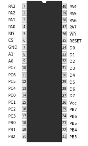
Image source: https://images.app.goo.gl/22BfM5mn9ZFo96S26
图片来源:https://images.app.goo.gl/22BfM5mn9ZFo96S26
Let us take a look at the functionalities of each of its pins,
让我们看一下其每个引脚的功能,
PA0 to PA1
PA0至PA1
These pins are the data lines for the port A. These pins are equally distributed on both sides of the top of the 8255 IC. The keys 1 to 4 and 37 to 40 are the pins devoted for port A.
这些引脚是端口A的数据线。这些引脚均匀分布在8255 IC顶部的两侧。 按键1至4和37至40是专用于端口A的引脚。
PB0 to PB1
PB0至PB1
These pins are the data lines for Port B and the keys 18 to 25 are the pins that carry the data of port B.
这些引脚是端口B的数据线,键18至25是承载端口B数据的引脚。
PC0 to PC1
PC0至PC1
These pins are the data lines for the port C. The keys 10 to 17 carry the data bits of port A. Among these, the pins 10 to 13 are the Port C upper pins, and 314 to 17 are the pins devoted for port C lower.
这些引脚是端口C的数据线。键10到17携带端口A的数据位。其中,引脚10到13是端口C的上引脚,而314到17是专用于端口C的引脚。降低。
D0 to D7
D0至D7
These pins carry the 8-bit binary code which is used to instruct the working of the entire IC. These pins together are called as the control word or control register. The keys 27 to 34 carry the contents of the control word.
这些引脚带有8位二进制代码,用于指示整个IC的工作。 这些引脚一起称为控制字或控制寄存器。 键27至34携带控制字的内容。
A0 and A1
A0和A1
These pins decide which port will be selected for transferring the data. These keys are present at pins 8 and 9.
这些引脚决定将选择哪个端口来传输数据。 这些键位于引脚8和9。
| A0 | A1 | Port selected |
|---|---|---|
| 0 | 0 | Port A |
| 0 | 1 | Port B |
| 1 | 0 | Port C |
| 1 | 1 | Control Register |
| A0 | A1 | 选择的端口 |
|---|---|---|
| 0 | 0 | 港口A |
| 0 | 1个 | 港口B |
| 1个 | 0 | C口 |
| 1个 | 1个 | 控制寄存器 |
RD'
RD'
It is an active low signal key which puts the IC in reading mode. It is present at key number 5.
这是一个有效的低信号键,可将IC置于读取模式。 它出现在键号5处。
WR'
WR'
It is an active low signal key which puts the IC in writing mode. It is present at key number 36.
这是一个有效的低信号键,可将IC置于写入模式。 它位于密钥号36处。
CS'
CS'
It is also an active low signal key which is responsible for chip selection. The key number 6 is devoted to chip select key.
它也是一个有效的低信号键,负责芯片选择。 键号6专用于片选键。
RESET
重启
This key present at 35 number when in set mode, resets the entire data present in all the keys to their default values.
在设置模式下,此键显示为35个数字,将所有键中显示的全部数据重置为其默认值。
GND
地线
There is one ground key for 8255 IC present at key number 7.
钥匙号7上有一个用于8255 IC的接地钥匙。
VCC
VCC
The VCC key is from where the IC receives the 5V input. It is present at the key 26.
VCC键是IC接收5V输入的地方。 它位于钥匙26上。
ppi280 ppi


 3584
3584

 被折叠的 条评论
为什么被折叠?
被折叠的 条评论
为什么被折叠?
 到【灌水乐园】发言


