


Some Examples of Transactions
This section describes a few transaction examples showing packets transmitted between requester and completer to accomplish a transaction. The examples consist of a memory read, IO write, and Memory write.
Memory Read Originated by CPU, Targeting an Endpoint
Figure 2-6 shows an example of packet routing associated with completing a memory read transaction. The root complex on the behalf of the CPU initiates a non-posted memory read from the completer endpoint shown. The root complex transmits an MRd packet which contains amongst other fields, an address, TLP type, requester ID (of the root complex) and length of transfer (in doublewords) field. Switch A which is a 3 port switch receives the packet on its upstream port. The switch logically appears like a 3 virtual bridge device connected by an internal bus. The logical bridges within the switch contain memory and IO base and limit address registers within their configuration space similar to PCI bridges. The MRd packet address is decoded by the switch and compared with the base/limit address range registers of the two downstream logical bridges. The switch internally forwards the MRd packet from the upstream ingress port to the correct downstream port (the left port in this example). The MRd packet is forwarded to switch B. Switch B decodes the address in a similar manner. Assume the MRd packets is forwarded to the right-hand port so that the completer endpoint receives the MRd packet.
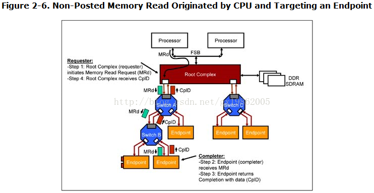
The completer decodes the contents of the header within the MRd packet, gathers the requested data and returns a completion packet with data (CplD). The header portion of the completion TLP contains the requester ID copied from the original request TLP. The requester ID is used to route the completion packet back to the root complex.
The logical bridges within Switch B compares the bus number field of the requester ID in the CplD packet with the secondary and subordinate bus number configuration registers. The CplD packet is forwarded to the appropriate port (in this case the upstream port). The CplD packet moves to Switch A which forwards the packet to the root complex. The requester ID field of the completion TLP matches the root complex's ID. The root complex checks the completion status (hopefully "successful completion") and accepts the data. This data is returned to the CPU in response to its pending memory read transaction.
Memory Read Originated by Endpoint, Targeting System Memory
In a similar manner, the endpoint device shown in Figure 2-7 on page 67 initiates a memory read request (MRd). This packet contains amongst other fields in the header, the endpoint's requester ID, targeted address and amount of data requested. It forwards the packet to Switch B which decodes the memory address in the packet and compares it with the memory base/limit address range registers within the virtual bridges of the switch. The packet is forwarded to Switch A which decodes the address in the packet and forwards the packet to the root complex completer.
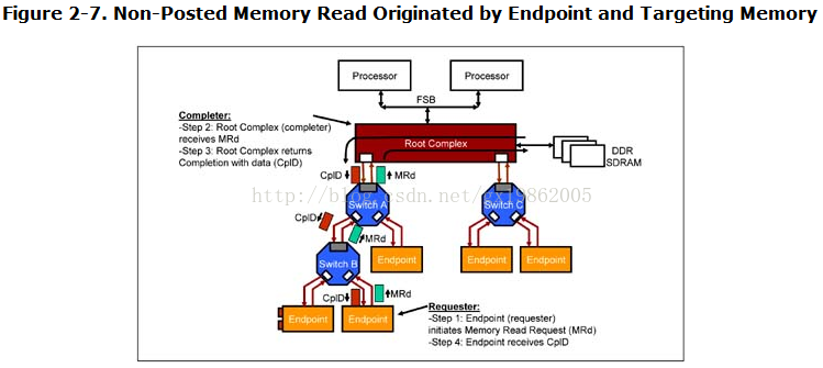
The root complex obtains the requested data from system memory and creates a completion TLP with data (CplD). The bus number portion of the requester ID in the completion TLP is used to route the packet through the switches to the endpoint.
A requester endpoint can also communicate with another peer completer endpoint. For example an endpoint attached to switch B can talk to an endpoint connected to switch C. The request TLP is routed using an address. The completion is routed using bus number. Multi-port root complex devices are not required to support port-to-port packet routing. In which case, peer-to-peer transactions between endpoints associated with two different ports of the root complex is not supported.
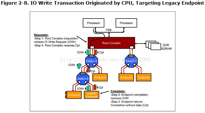
IO requests can only be initiated by a root complex or a legacy endpoint. PCI Express endpoints do not initiate IO transactions. IO transactions are intended for legacy support. Native PCI Express devices are not prohibited from implementing IO space, but the specification states that a PCI Express Endpoint must not depend on the operating system allocating I/O resources that are requested.
IO requests are routed by switches in a similar manner to memory requests. Switches route IO request packets by comparing the IO address in the packet with the IO base and limit address range registers in the virtual bridge configuration space associated with a switch
Figure 2-8 on page 68 shows routing of packets associated with an IO write transaction. The CPU initiates an IO write on the Front Side Bus (FSB). The write contains a target IO address and up to 4 Bytes of data. The root complex creates an IO Write request TLP (IOWr) using address and data from the CPU transaction. It uses its own requester ID in the packet header. This packet is routed through switch A and B. The completer endpoint returns a completion without data (Cpl) and completion status of 'successful completion' to confirm the reception of good data from the requester.
Memory Write Transaction Originated by CPU and Targeting an Endpoint
Memory write (MWr) requests (and message requests Msg or MsgD) are posted transactions. This implies that the completer does not return a completion. The MWr packet is routed through the PCI Express fabric of switches in the same manner as described for memory read requests. The requester root complex can write up to 4 KBytes of data with one MWr packet.
Figure 2-9 on page 69 shows a memory write transaction originated by the CPU. The root complex creates a MWr TLP on behalf of the CPU using target address and data from the CPU FSB transaction. This packet is routed through switch A and B. The packet reaches the endpoint and the transaction is complete.

PCI Transaction Model - Programmed IO
Consider an example in which the CPU communicates with a PCI peripheral such as an Ethernet device shown inFigure 1-5. Transaction 1 shown in the figure, which is initiated by the CPU and targets a peripheral device, is referred to as a programmed IO transaction. Software commands the CPU to initiate a memory or IO read/write bus cycle on the host bus targeting an address mapped in a PCI device's address space. The North bridge arbitrates for use of the PCI bus and when it wins ownership of the bus generates a PCI memory or IO read/write bus cycle. During the first clock of this bus cycle (known as the address phase), all target devices decode the address. One target (the Ethernet device in this example) decodes the address and claims the transaction. The master (North bridge in this case) communicates with the claiming target (Ethernet controller). Data is transferred between master and target in subsequent clocks after the address phase of the bus cycle. Either 4 bytes or 8 bytes of data are transferred per clock tick depending on the PCI bus width. The bus cycle is referred to as a burst bus cycle if data is transferred back-to-back between master and target during multiple data phases of that bus cycle. Burst bus cycles result in the most efficient use of PCI bus bandwidth.

At 33 MHz and the bus width of 32-bits (4 Bytes), peak bandwidth achievable is 4 Bytes x 33 MHz = 133 MBytes/sec. Peak bandwidth on a 64-bit bus is 266 Mbytes/sec. SeeTable 1-2 on page 13.
Efficiency of the PCI bus for data payload transport is in the order of 50%. Efficiency is defined as number of clocks during which data is transferred divided by the number of total clocks, times 100. The lost performance is due to bus idle time between bus cycles, arbitration time, time lost in the address phase of a bus cycle, wait states during data phases, delays during transaction retries (not discussed yet), as well as latencies through PCI bridges.
PCI Transaction Model - Direct Memory Access (DMA)
Data transfer between a PCI device and system memory is accomplished in two ways:
The first less efficient method uses programmed IO transfers as discussed in the previous section. The PCI device generates an interrupt to inform the CPU that it needs data transferred. The device interrupt service routine (ISR) causes the CPU to read from the PCI device into one of its own registers. The ISR then tells the CPU to write from its register to memory. Similarly, if data is to be moved from memory to the PCI device, the ISR tells the CPU to read from memory into its own register. The ISR then tells the CPU to write from its register to the PCI device. It is apparent that the process is very inefficient for two reasons. First, there are two bus cycles generated by the CPU for every data transfer, one to memory and one to the PCI device. Second, the CPU is busy transferring data rather than performing its primary function of executing application code.
The second more efficient method to transfer data is the DMA (direct memory access) method illustrated by Transaction 2 inFigure 1-5 on page 20, where the PCI device becomes a bus master.Upon command by a local application (software) which runs on a PCI peripheral or the PCI peripheral hardware itself, the PCI device may initiate a bus cycle to talk to memory. The PCI bus master device (SCSI device in this example) arbitrates for the PCI bus, wins ownership of the bus and initiates a PCI memory bus cycle. The North bridge which decodes the address acts as the target for the transaction. In the data phase of the bus cycle, data is transferred between the SCSI master and the North bridge target. The bridge in turn generates a DRAM bus cycle to communicate with system memory. The PCI peripheral generates an interrupt to inform the system software that the data transfer has completed. This bus master or DMA method of data transport is more efficient because the CPU is not involved in the data move and further only one burst bus cycle is generated to move a block of data.
So DMA transfer is between North Bridge and Endpoint device, not between DRAM and Endpoint device. North Bridge generates DRAM bus cycle to communicate with system memory to get related data, then transfer the data to Endpoint device through DMA.
Apparently, DMA is hardware implement while programmed IO transfer is software implement. Actually DMA hardcode the software implement in the device core. so for DMA the transfer job is done by hardware instead of software. No matter DMA or software, a lot of job is needed to do, such as retry if there's error.
DMA is part of Device core layer as below Figure 2-10. Meanwhile there's advanced DMA called Scatter-Gather DMA, take Disk for example, struct bio describes continuous blocks in disk but scattered segments in memory, in this situation, Scatter-Gather DMA can do a great job.
PCI Express Device Layers
OverviewThe PCI Express specification defines a layered architecture for device design as shown inFigure 2-10 on page 70. The layers consist of a Transaction Layer, a Data Link Layer and a Physical layer. The layers can be further divided vertically into two, a transmit portion that processes outbound traffic and a receive portion that processes inbound traffic. However, a device design does not have to implement a layered architecture as long as the functionality required by the specification is supported.
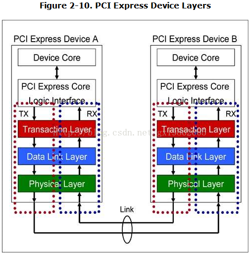
Device Core / Software Layer
The Device Core consists of, for example, the root complex core logic or an endpoint core logic such as that of an Ethernet controller, SCSI controller, USB controller, etc. To design a PCI Express endpoint, a designer may reuse the Device Core logic from a PCI or PCI-X core logic design and wrap around it the PCI Express layered design described in this section.
Transmit Side
The Device Core logic in conjunction with local software provides the necessary information required by the PCI Express device to generate TLPs. This information is sent via the Transmit interface to the Transaction Layer of the device.Example of information transmitted to the Transaction Layer includes: transaction type to inform the Transaction Layer what type of TLP to generate, address, amount of data to transfer, data, traffic class, message index etc.
Receive Side
The Device Core logic is also responsible to receive information sent by the Transaction Layer via the Receive interface.This information includes: type of TLP received by the Transaction Layer, address, amount of data received, data, traffic class of received TLP, message index, error conditions etc.


 3080
3080

 被折叠的 条评论
为什么被折叠?
被折叠的 条评论
为什么被折叠?
 到【灌水乐园】发言


