


第15节 SRIO例程
参考文档:(系列博客,对官方SRIO手册的中文解释)
https://blog.csdn.net/kunkliu/article/details/105271629
创龙提供的SRIO中文参考资料《C66x串行快速输入输出(SRIO)用户指南.pdf》
TI官方资料《Serial Rapid IO (SRIO) User Guide.pdf》
15.1节 K1_STK_v1.1回环测试例程
K1_STK_v1.1 中参考文档:(建议看一下)
《KeyStone_1_SRIO_STK_User's_Guide.doc》---理解SRIO回环测试原理
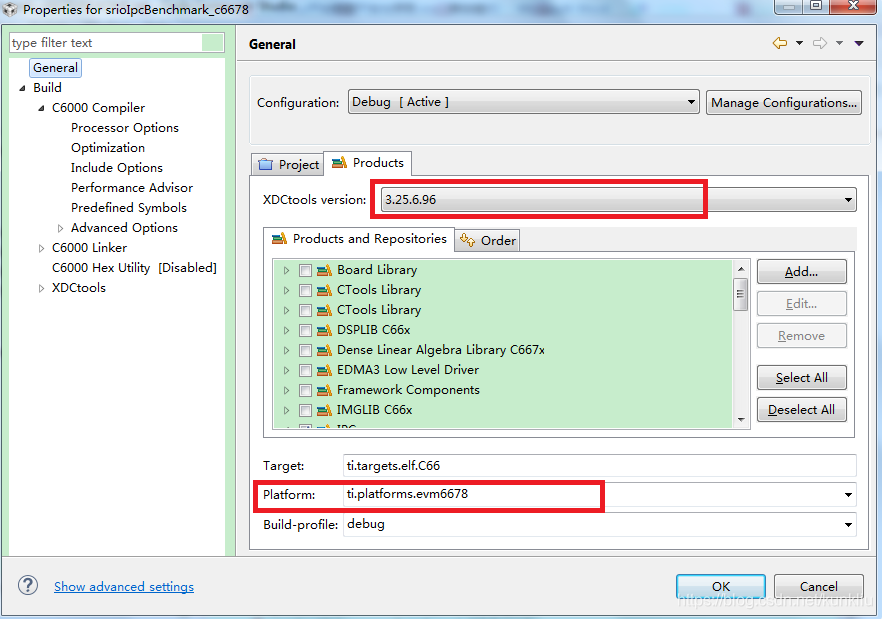
15.1.1 仿真不能定位到main函数
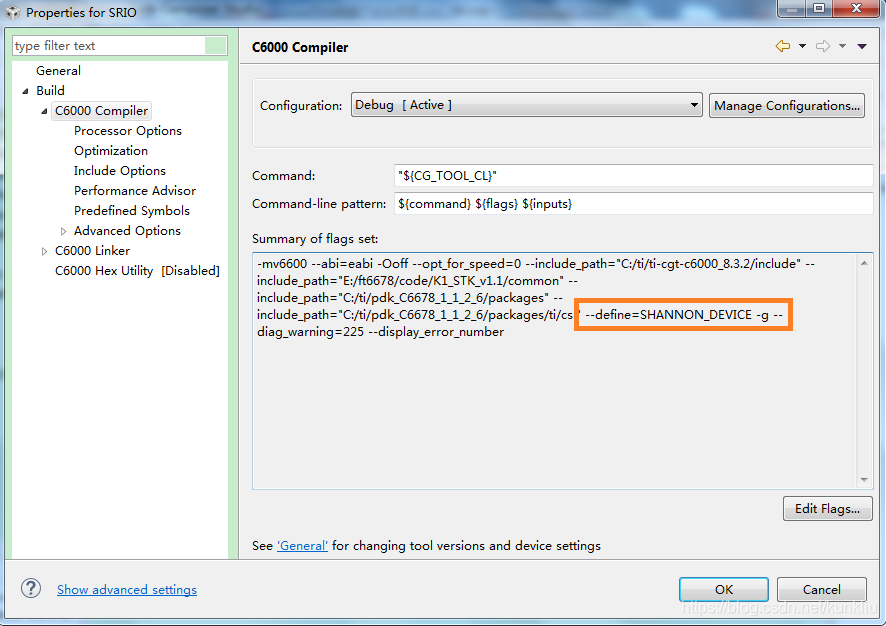
- 下图的platform和XDCtools有直接关系,版本要对应
15.2节 回环测试方法
- Digital loopback Test(外部不需要接线)
- Serdes loopback test(外部不需要接线)
- External loopback test(外部需要接线)

15.3节 创龙例程SYSBIOS_SRIO_Device01分析
- 硬件信息介绍
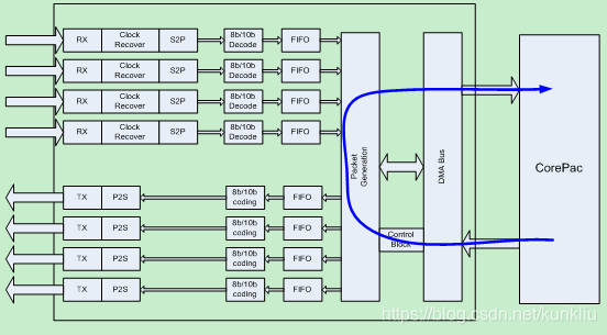
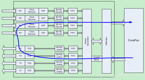
板卡上有4颗DSP6678,每颗6678的SRIO连接到桥片1848。
- 工程介绍
SYSBIOS_SRIO_Device01与SYSBIOS_SRIO_Device02配合使用完成SRIO数据传输,Device01主动向Device02 Nwrite写数据,Device02通过写数据的最后一个字节判断是否Nwrite完成,然后Device02将收到的数据乘10后,将数据通过Nwrite写回到Device01,Device01也通过写数据的最后一个字节判断是否Nwrite完成,循环上述过程。
- 工程编译
/*
 * CCSv7 IDE
 * 7.4
 *
 * 依赖组件版本为
 * - XDCTools 3.50.5.12-core *
 * - NDK 2.25.1.11 *
 * - SYS/BIOS 6.52.0.12 *
 * - UIA 2.20.0.02 *
 * - Tronlong.DSP.C6000.C66x
 */
- SRIO初始化代码如下:
void SRIOInit()
{
// 使能外设
PSCModuleControl(SOC_PSC_0_REGS, HW_PSC_SRIO, PSC_MDCTL_NEXT_ENABLE, PSC_POWERDOMAIN_SRIO, PSC_PDCTL_NEXT_ON);
// 禁用 SRIO 及 SRIO Block
SRIOGlobalDisable();
int i;
for(i = 0; i <= 9; i++)
{
SRIOBlockDisable(i);
}
// 设置 Boot Complete 为 0 以便可以修改 SRIO 所有寄存器包括只读(Read Only)寄存器
SRIOBootCompleteSet(SRIO_Disable);
// 使能 SRIO 及 SRIO Block
SRIOGlobalEnable();
for(i = 0; i <= 9; i++)
{
SRIOBlockEnable(i);
}
// 配置 SRIO Lane 工作模式
SRIOModeSet(0, SRIO_Normal);
SRIOModeSet(1, SRIO_Normal);
SRIOModeSet(2, SRIO_Normal);
SRIOModeSet(3, SRIO_Normal);
// 使能自动优先级提升
SRIOAutomaticPriorityPromotionEnable();
// 设置 SRIO VBUS 预分频为 44.7 到 89.5
SRIOPrescalarSelectSet(0);
// 解锁关键寄存器
KickUnlock();
// 配置 SRIO SerDes 时钟(156.25Mhz x 16 = 2.5GHz)
SRIOSerDesPLLSet(0x81); // 5G
// 配置 SRIO SerDes 发送 / 接收
// 数据率 5Gbps(8B/10B)
SRIOSerDesTxSet(0, 0x001C8F95); //0x00180795 0x001C8F95
SRIOSerDesTxSet(1, 0x001C8F95);
SRIOSerDesTxSet(2, 0x001C8F95);
SRIOSerDesTxSet(3, 0x001C8F95);
SRIOSerDesRxSet(0, 0x00468495); //0x00440495 0x00468495
SRIOSerDesRxSet(1, 0x00468495);
SRIOSerDesRxSet(2, 0x00468495);
SRIOSerDesRxSet(3, 0x00468495);
// 等待 SRIO SerDes 锁定
while(!(SRIOSerDesPLLStatus() & 0x1));
// 锁定关键寄存器
KickLock();
// 设置设备信息
SRIODeviceInfoSet(DEVICE_ID1_8BIT, 0x50, DEVICE_REVISION);
// 设置组织信息
SRIOAssemblyInfoSet(DEVICE_ASSEMBLY_ID, DEVICE_ASSEMBLY_VENDOR_ID, DEVICE_ASSEMBLY_REVISION, DEVICE_ASSEMBLY_INFO);
// PE 特性配置
SRIOProcessingElementFeaturesSet(0x20000199);
// 配置源及目标操作
SRIODestinationOperationsSet(0x0004FDF4);
SRIODestinationOperationsSet(0x0000FC04);
// 设置 SRIO 设备 ID
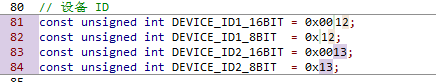
SRIODeviceIDSet(DEVICE_ID1_8BIT, DEVICE_ID1_16BIT);
// 配置 TLM 基本路由信息
SRIOTLMPortBaseRoutingSet(SRIO_Port0, 1, SRIO_Enable, SRIO_Enable, SRIO_Disable);
SRIOTLMPortBaseRoutingPatternMatchSet(SRIO_Port0, 1, DEVICE_ID2_8BIT, 0xFF);
// 配置端口 PLM
// 配置 PLM 端口 Silence Timer
SRIOPLMPortSilenceTimerSet(SRIO_Port0, 0x2);
// 使能端口
SRIOInputPortEnable(SRIO_Port0);
SRIOOutputPortEnable(SRIO_Port0);
// 配置 PLM 端口 Discovery Timer
SRIOPLMPortDiscoveryTimerSet(SRIO_Port0, 0x2);
// 配置端口 Write Reception Capture
SRIOPortWriteRxCapture(SRIO_Port0, 0x0);
// 配置端口连接超时
SRIOPortLinkTimeoutSet(0x000FFF);
// 端口 Master 使能
SRIOPortGeneralSet(SRIO_Enable, SRIO_Enable, SRIO_Disable);
// 清除 Sticky Register 位
SRIORegisterResetControlClear();
// 设置端口写 ID
SRIOPortWriteTargetDeviceID(0, DEVICE_ID2_8BIT, SRIO_ID_8Bit);
// 设置数据流最大传输单元(MTU)
SRIODataDtreamingLogicalLayerControl(64);
// 配置端口路由模式
SRIOPLMPathModeControl(SRIO_Port0, SRIO_Mode4_1_4x);
// 设置 LLM Port IP 预分频
SRIOServerClockPortIPPrescalar(0x1F);
// 使能外设
SRIOPeripheralEnable();
// 配置完成
SRIOBootCompleteSet(SRIO_Enable);
// 检查端口是否就绪
while(SRIOPortOKCheck(SRIO_Port0) != TRUE);
}
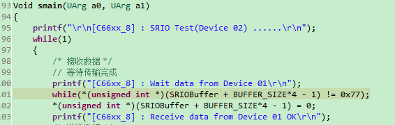
- main函数中接收数据部分代码,以Device02介绍
- 程序运行方法:
- 将SYSBIOS_SRIO_Device01加载到dsp0的0核,SYSBIOS_SRIO_Device02加载到dsp1 的0核
- 先运行dsp1的SYSBIOS_SRIO_Device02,在运行dsp0的SYSBIOS_SRIO_Device01
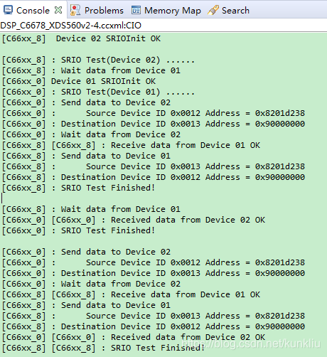
- console打印信息如下:
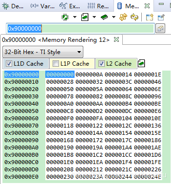
- device01 与device02的0x90000000内存值均为如下图:
15.4节 创龙例程SYSBIOS_SRIO_Device01v2分析
在上一节基础上增加了门铃的代码。调了好久才把门铃调通,SYSBIOS_SRIO_Device01v2与SYSBIOS_SRIO_Device02v2修改部分基本一致,下面将修改部分一一列出:
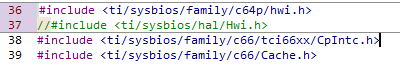
- cfg文件修改:
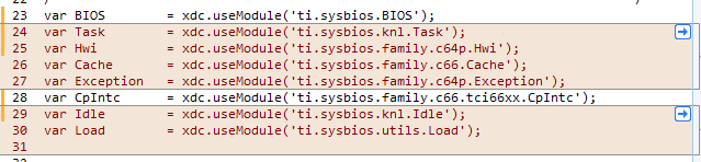
对应包含的头文件修改如下:
- SRIOInit初始化代码如下:
void SRIOInit()
{
// 使能外设
PSCModuleControl(SOC_PSC_0_REGS, HW_PSC_SRIO, PSC_MDCTL_NEXT_ENABLE, PSC_POWERDOMAIN_SRIO, PSC_PDCTL_NEXT_ON);
// 禁用 SRIO 及 SRIO Block
SRIOGlobalDisable();
int i;
for(i = 0; i <= 9; i++)
{
SRIOBlockDisable(i);
}
// 设置 Boot Complete 为 0 以便可以修改 SRIO 所有寄存器包括只读(Read Only)寄存器
SRIOBootCompleteSet(SRIO_Disable);
// 使能 SRIO 及 SRIO Block
SRIOGlobalEnable();
for(i = 0; i <= 9; i++)
{
SRIOBlockEnable(i);
}
// 配置 SRIO Lane 工作模式
SRIOModeSet(0, SRIO_Normal);
SRIOModeSet(1, SRIO_Normal);
SRIOModeSet(2, SRIO_Normal);
SRIOModeSet(3, SRIO_Normal);
// 使能自动优先级提升
SRIOAutomaticPriorityPromotionEnable();
// 设置 SRIO VBUS 预分频为 44.7 到 89.5
SRIOPrescalarSelectSet(0);
// 解锁关键寄存器
KickUnlock();
// 配置 SRIO SerDes 时钟(156.25Mhz x 16 = 2.5GHz)
SRIOSerDesPLLSet(0x81); // 5G
// 配置 SRIO SerDes 发送 / 接收
// 数据率 5Gbps(8B/10B)
SRIOSerDesTxSet(0, 0x001C8F95);
SRIOSerDesTxSet(1, 0x001C8F95);
SRIOSerDesTxSet(2, 0x001C8F95);
SRIOSerDesTxSet(3, 0x001C8F95);
SRIOSerDesRxSet(0, 0x00468495);
SRIOSerDesRxSet(1, 0x00468495);
SRIOSerDesRxSet(2, 0x00468495);
SRIOSerDesRxSet(3, 0x00468495);
// 等待 SRIO SerDes 锁定
while(!(SRIOSerDesPLLStatus() & 0x1));
// 锁定关键寄存器
KickLock();
// 设置设备信息
SRIODeviceInfoSet(DEVICE_ID1_8BIT, 0x50, DEVICE_REVISION);
// 设置组织信息
SRIOAssemblyInfoSet(DEVICE_ASSEMBLY_ID, DEVICE_ASSEMBLY_VENDOR_ID, DEVICE_ASSEMBLY_REVISION, DEVICE_ASSEMBLY_INFO);
// PE 特性配置
SRIOProcessingElementFeaturesSet(0x20000199);
// 配置源及目标操作
SRIOSourceOperationsSet(0x0004FDF4);
SRIODestinationOperationsSet(0x0000FC04);
// 设置 SRIO 设备 ID
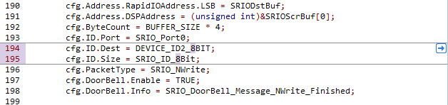
SRIODeviceIDSet(DEVICE_ID1_8BIT, DEVICE_ID1_16BIT);
// 配置 TLM 基本路由信息
SRIOTLMPortBaseRoutingSet(SRIO_Port0, 1, SRIO_Enable, SRIO_Enable, SRIO_Disable);
SRIOTLMPortBaseRoutingPatternMatchSet(SRIO_Port0, 1, DEVICE_ID2_8BIT, 0xFF);
// 配置端口 PLM
// 配置 PLM 端口 Silence Timer
SRIOPLMPortSilenceTimerSet(SRIO_Port0, 0x2);
// 使能端口
SRIOInputPortEnable(SRIO_Port0);
SRIOOutputPortEnable(SRIO_Port0);
// 配置 PLM 端口 Discovery Timer
SRIOPLMPortDiscoveryTimerSet(SRIO_Port0, 0x2);
// 配置端口 Write Reception Capture
SRIOPortWriteRxCapture(SRIO_Port0, 0x0);
// 配置端口连接超时
SRIOPortLinkTimeoutSet(0x000FFF);
// 端口 Master 使能
SRIOPortGeneralSet(SRIO_Enable, SRIO_Enable, SRIO_Disable);//实验发现必须第一个参数为enable,门铃才能中断,目前不知道原因何在
// 清除 Sticky Register 位
SRIORegisterResetControlClear();
// 设置端口写 ID
SRIOPortWriteTargetDeviceID(0, DEVICE_ID2_8BIT, SRIO_ID_8Bit);
// 设置数据流最大传输单元(MTU)
SRIODataDtreamingLogicalLayerControl(64);
// 配置端口路由模式
SRIOPLMPathModeControl(SRIO_Port0, SRIO_Mode4_1_4x);
// 设置 LLM Port IP 预分频
SRIOServerClockPortIPPrescalar(0x1F);
// DoorBell 中断配置
SRIODoorBellInterruptRoutingControl(SRIO_DoorBell_Dedicated_INT);
// DoorBell 中断路由配置
SRIODoorBellInterruptConditionRoutingSet(SRIO_DoorBell0, SRIO_DoorBellInt0, SRIO_IntDst_0_16);
SRIODoorBellInterruptConditionRoutingSet(SRIO_DoorBell0, SRIO_DoorBellInt1, SRIO_IntDst_0_16);
SRIODoorBellInterruptConditionRoutingSet(SRIO_DoorBell0, SRIO_DoorBellInt2, SRIO_IntDst_0_16);
SRIODoorBellInterruptConditionRoutingSet(SRIO_DoorBell0, SRIO_DoorBellInt3, SRIO_IntDst_0_16);
// 使能外设
SRIOPeripheralEnable();
// 配置完成
SRIOBootCompleteSet(SRIO_Enable);
}
- main.c修改如下:
main.c基本应用逻辑没有修改,只是增加了一些打印信息,方便调试。主要修改点为,将SRIO DEVICE ID修改为了8 位的,对应发送接受配置时,ID的修改,此处不在一一列出。
- 应用层逻辑如下:
- Device01v2和Device01v2启动后分别创建SRIODoorBellIsr、DoorBellIntTsk和smain。
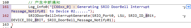
- Device01v2为主动发起者,启动后,SRIODoorBellIsr等待2.5s后,向Device02v2发送SRIO_DoorBell_Message_Notify01门铃中断。
- Device02v2收到门铃后,在中断函数中向DoorBellIntTsk发送信号量sem1,促使原先阻塞的DoorBellIntTsk运行,并向Device01v2发送SRIO_DoorBell_Message_Notify00门铃中断。
- Device01v2收到门铃后,在中断函数中向smain发送信号量sem,促使原先阻塞的smain运行,初始化发送数据,并向Device02v2发送SRIO_NWrite并且带有门铃,门铃类型为SRIO_DoorBell_Message_NWrite_Finished(此处没有明白为什么NWrite能和doorbell一起发送),然后smain又阻塞在sem信号量上。
- Device02v2此时能够收到Device01v2 NWrite的数据,又能够产生门铃中断,并在中断函数中发出sem信号量,促使原先阻塞的smain运行,然后将收到的数据乘10后,将数据向Device01v2发送SRIO_NWrite并且带有门铃,门铃类型为SRIO_DoorBell_Message_NWrite_Finished,smain执行完成。
- Device01v2能够收到Device02v2 NWrite的数据,产生门铃中断,并在中断函数中发出sem信号量,促使原先阻塞的smain运行,对发送的数据与接收的数据比较,smain执行完成。
原本很简单的通讯流程被我写的有点繁琐。不过门铃工程中中断与信号量的配合使用还是值得学习的。
- 程序运行方法:
- 将SYSBIOS_SRIO_Device01v2加载到dsp0的0核,SYSBIOS_SRIO_Device02v2加载到dsp1 的0核
- 先运行dsp1的SYSBIOS_SRIO_Device02v2,在运行dsp0的SYSBIOS_SRIO_Device01v2
- console打印信息如下:
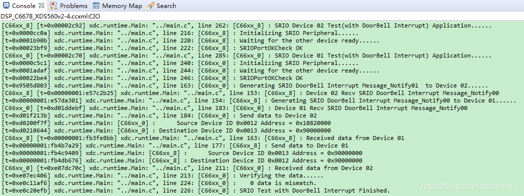
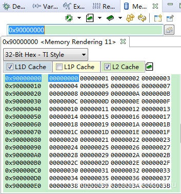
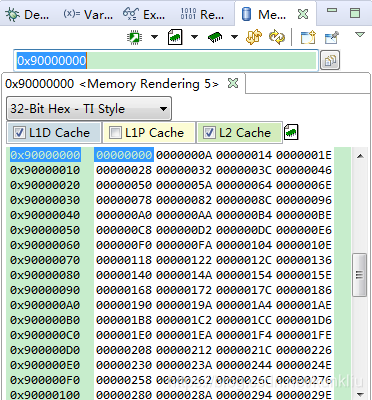
- device01 与device02的0x90000000内存值均为如下图:


 1295
1295

 被折叠的 条评论
为什么被折叠?
被折叠的 条评论
为什么被折叠?
 到【灌水乐园】发言


