


1 TRANSMISSION GATE
1.1 Introduction
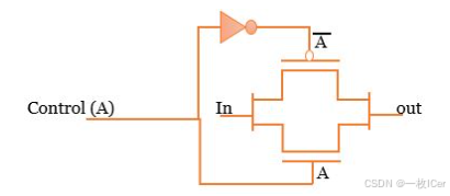
A transmission gate, or analog switch, is defined as an electronic element that will selectively block or pass a signal level from the input to the output. This solid-state switch is comprised of a parallel connection of pMOS transistor and nMOS transistor. The control gates are biased in a complementary manner so that both transistors are either on or off.
The schematic diagram (Fig.1) includes the arbitrary labels for IN and OUT, as the circuit will operate in an identical manner if those labels were reversed. This design provides true bidirectional connectivity without degradation of the input signal.
1.2 Truth Table
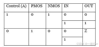
Note: PMOS is on when gate input is 0. NMOS is on when gate input is 1.
1.3 Working mechanism
From the truth table we can see When control is high (1) both transistors are ON at the same time and whatever is applied to the input will arrive at the output.
From the truth table we can see When control is low (0) both transistors are OFF at the same time and whatever is applied to the input will arrive at the output, so we get high impedance (Z) at the output.
2 D latch
2.1 Introduction
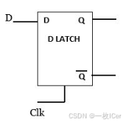
The latch is a level-sensitive device. In a latch the output (Q) is dependent only on the level of the clock (Clk). (Fig.2)
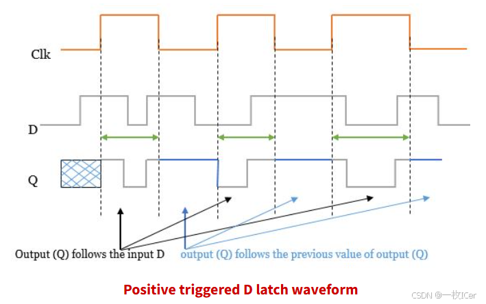
If it is a positive level-sensitive latch. It is transparent that when the clock is high, Output (Q) follows the input D. Otherwise, output (Q) follows the previous value of output (Q).The waveform below (Fig.3) is an example.
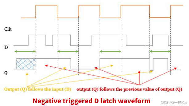
If it is a negative level-sensitive latch, when the clock is low, Output (Q) follows the input D. Otherwise, output (Q) follows the previous value of output (Q). The waveform below (Fig.4) is an example.
2.2 Internal Structure
2.2.1 Positive D latch using transmission Gate
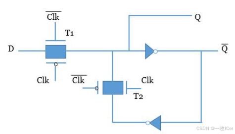
It consists of two transmission gates and two inverters. The composition of latch is shown in Fig.5
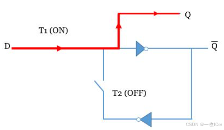
When Clk = high (1) T1 is ON and T2 is OFF, so output (Q) directly follows the input (D). (Fig.6)
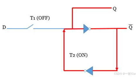
When Clk = low (0) T1 is OFF and T2 is ON, now new data entering into the latch is stopped and we get only previously-stored data at the output. (Fig.7)
2.2.2 Negative D latch using transmission Gate
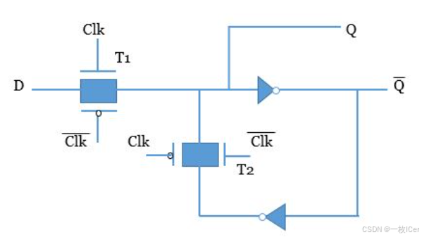
It is also consist of two transmission gate and two inverters. It is working in an exactly opposite manner of the positive level-sensitive D latch. The composition of Negative D latch is shown in Fig.8
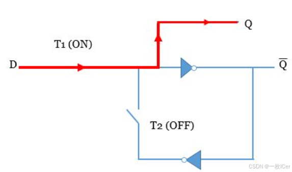
When Clk = low (0) T1 is ON and T2 is OFF, so output (Q) directly follows the input (D). (Fig.9)
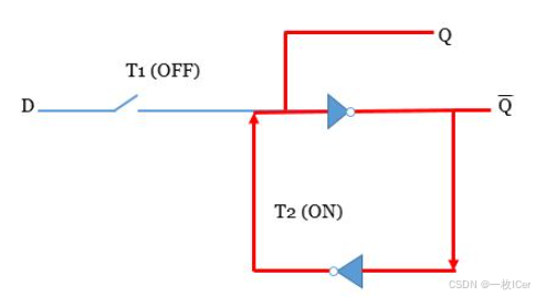
When Clk = high (1) T1 is OFF and T2 is ON, now new data entering into the latch is stopped and we get only previously-stored data at the output. (Fig.10)
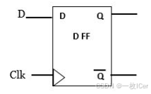
3 D Flip Flop
3.1 Introduction
A D flip flop is an edge-triggered device which means the output (Q) follows the input (D) only at the active edge (for positive rising edge) of the clock (for the positive edge-triggered) and retain the same value until the next rising edge i.e. output does not change between two rising edges, it should be changed only at the rising edge. (Fig.11)
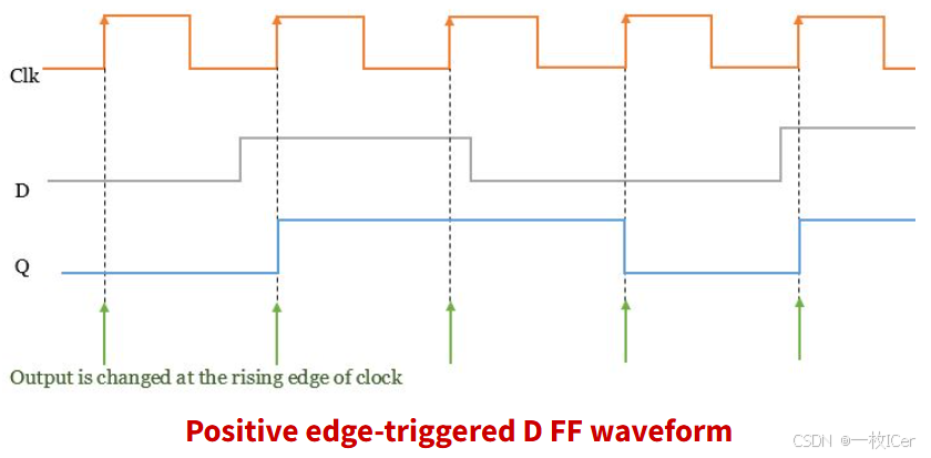
If it is a Positive edge-triggered D FF waveform, output is changed at the rising edge of clock.(Fig.12)
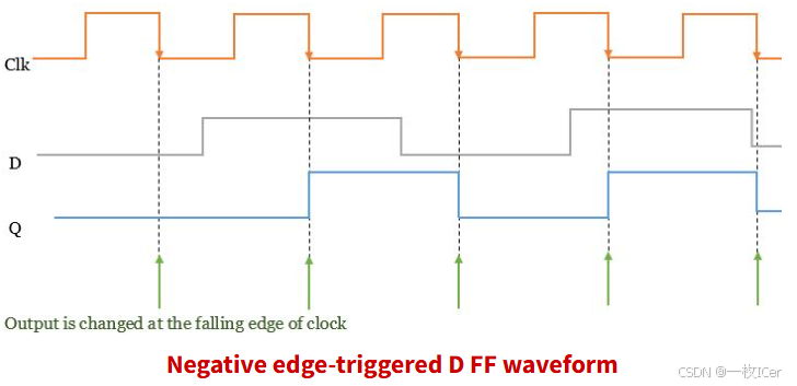
If it is a Negative edge-triggered D FF waveform, output is changed at the falling edge of clock.(Fig.13)
3.2 Working mechanism
In the next chapters, We will mainly analyze the Positive edge-triggered D FF using Transmission gate.
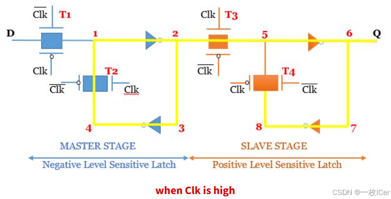
D FF is a combination of negative level-sensitive latch and positive level-sensitive latch that giving an edge-sensitive device. Data is change only at the active edge of the clock. The composition of a D FF is shown in Fig.14.
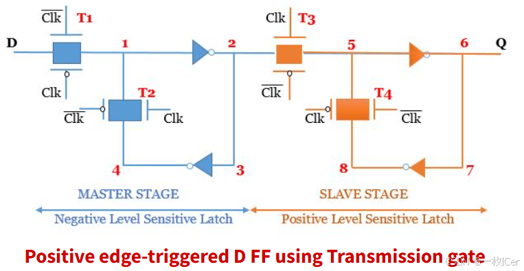
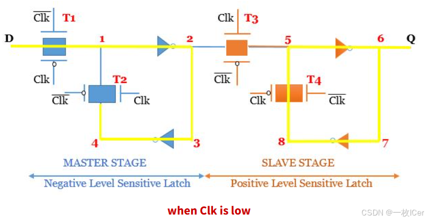
When Clk = LOW(0), T1, T4 is ON and T2, T3 is OFF.
For the master latch, New data (D) is continuously entering through T1 and getting stored till the edge of T2 (path is D-1-2-3-4 and at node 4 it stops). It cannot pass through T2 and T3 transmission gate because they are off.
For the slave latch, it keeps retaining the previously stored value of output (Q) (path is 5-6-7-8-5).
These paths are shown in Fig.15.
When Clk = HIGH (1) T2, T3 are ON and T1, T4 are OFF.
For the master latch, the master latch did not allow new data to enter into the device because T1 is OFF and the previously stored data at point 4 is going through the path 4-1-2-5-6-Q and this same data is reflected at the output and this does not change until the next rising edge and this same data is also going to the transmission gate T4 (path is 4-1-2-5-6-7-8 and stops because transmission gate T4 is OFF). These paths are shown in Fig.16.
3.3 Conclusion
Again if Clk is low the master latching circuit is enabled and there is no change in the output. Any changes in input is reflected at node 4 which is reflected at the output at the next positive edge of the clock.
So we can say that if D changes, the changes would reflect only at node 4 when the clock is low and it will appear at the output only when the Clk is high.


 被折叠的 条评论
为什么被折叠?
被折叠的 条评论
为什么被折叠?
 到【灌水乐园】发言


