


目录
Dff
A D flip-flop is a circuit that stores a bit and is updated periodically, at the (usually) positive edge of a clock signal.
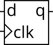
D flip-flops are created by the logic synthesizer when a clocked always block is used (See alwaysblock2). A D flip-flop is the simplest form of "blob of combinational logic followed by a flip-flop" where the combinational logic portion is just a wire.
Create a single D flip-flop.
Write your solution here
module top_module (
    input clk,    // Clocks are used in sequential circuits
    input d,
    output reg q );//

    // Use a clocked always block
    //   copy d to q at every positive edge of clk
    always@(posedge clk)
        q <=d;//时钟使用非阻塞赋值
    //   Clocked always blocks should use non-blocking assignments

endmodule
Dff8
Create 8 D flip-flops. All DFFs should be triggered by the positive edge of clk.
Write your solution here
module top_module (
    input clk,
    input [7:0] d,
    output [7:0] q
);

endmodule
Dff8r
Create 8 D flip-flops with active high synchronous reset. All DFFs should be triggered by the positive edge of clk.
Write your solution here
module top_module (
    input clk,
    input reset,            // Synchronous reset
    input [7:0] d,
    output [7:0] q
);

    always@(posedge clk)//同步复位
        if(reset == 1'b1)
            q<=8'h0000;
        else
            q<=d;
endmodule
Dff8p
Create 8 D flip-flops with active high synchronous reset. The flip-flops must be reset to 0x34 rather than zero. All DFFs should be triggered by the negative edge of clk.
Write your solution here
module top_module (
    input clk,
    input reset,
    input [7:0] d,
    output [7:0] q
);

    always@(negedge clk)
        if(reset == 1'b1)
            q<=8'h34;//0x34(16进制)== 0011 0100
        else
            q<=d;

endmodule
Dff8ar
Create 8 D flip-flops with active high asynchronous reset. All DFFs should be triggered by the positive edge of clk.
Write your solution here
module top_module (
    input clk,
    input areset,   // active high asynchronous reset
    input [7:0] d,
    output [7:0] q
);
    always@(posedge clk or posedge areset)//异步复位
    //复位信号不受时钟的控制,只要复位信号有效,那么电路就会复位。
        if(areset)
                q<=8'h0000;
        else
            q<=d;

endmodule
Dff16e
Create 16 D flip-flops. It's sometimes useful to only modify parts of a group of flip-flops. The byte-enable inputs control whether each byte of the 16 registers should be written to on that cycle. byteena[1] controls the upper byte d[15:8], while byteena[0] controls the lower byte d[7:0].
resetn is a synchronous, active-low reset.
All DFFs should be triggered by the positive edge of clk.
Write your solution here
module top_module (
    input clk,
    input resetn,
    input [1:0] byteena,
    input [15:0] d,
    output [15:0] q
);
    always@(posedge clk)
        if(resetn == 1'b0)//resetn 带n表示低点位有效
            q<=16'h0;
    	else begin
            if(byteena[1] == 1'b1)
                q[15:8]<=d[15:8];
    		if(byteena[0] == 1'b1)
                q[7:0]<=d[7:0];
        end

endmodule
Exams/m2014 q4a
Implement the following circuit:

Note that this is a latch, so a Quartus warning about having inferred a latch is expected.
Write your solution here
module top_module (
    input d,
    input ena,
    output q);
	//D Latch(D锁存器)
    //= 0时,输出状态保持不变; = 1时,输出随输入状态而改变
    always@(*)
        if(ena)
            q<=d;
    	else
            q<=q;
endmodule
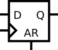
Exams/m2014 q4b
Implement the following circuit:
Write your solution here
module top_module (
    input clk,
    input d,
    input ar,   // asynchronous reset 异步复位
    output q);
//AR 代表 异步复位
    always@(posedge clk or posedge ar)
        if(ar)
            //该语句 if(ar)中的条件操作数为“ar”;若always中的“ar”是选择下降沿触发(negedge ar)。
            //下降沿触发的话,if()语句应该改为if(!ar)才对。
            //同理上升沿对应if()语句为if(ar)
            q<=0;
   	 	else
        	q<=d;
endmodule
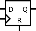
Exams/m2014 q4c
Implement the following circuit:
Write your solution here
module top_module (
    input clk,
    input d,
    input r,   // synchronous reset 同步复位
    output q);

    always@(posedge clk)
        if(r)
            q<=0;
    	else
            q<=d;
endmodule
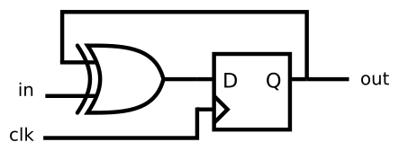
Exams/m2014 q4d
Implement the following circuit:
Write your solution here
module top_module (
    input clk,
    input in,
    output out);

    wire in1;
    assign in1=out^in;
    always@(posedge clk)
        out<=in1;

endmodule
Mt2015 muxdff
Taken from ECE253 2015 midterm question 5
Consider the sequential circuit below:
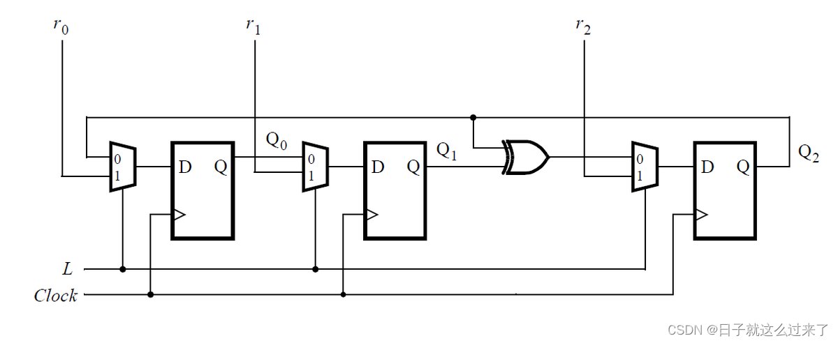
Assume that you want to implement hierarchical Verilog code for this circuit, using three instantiations of a submodule that has a flip-flop and multiplexer in it. Write a Verilog module (containing one flip-flop and multiplexer) named top_module for this submodule.
Write your solution here
module top_module (
	input clk,
	input L,
	input r_in,
	input q_in,
	output reg Q);

    always@(posedge clk)
        if(L)
            Q<=r_in;
    	else
            Q<=q_in;
endmodule
Exams/2014 q4a
Consider the n-bit shift register circuit shown below:
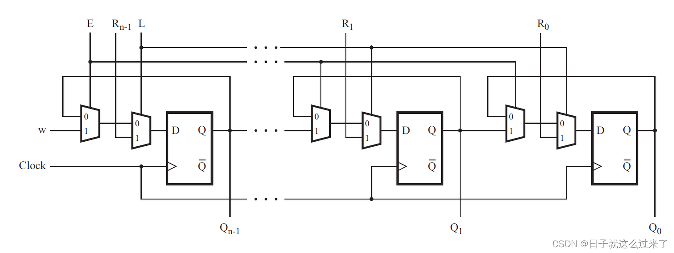
Write a Verilog module named top_module for one stage of this circuit, including both the flip-flop and multiplexers.
Write your solution here
module top_module (
    input clk,
    input w, R, E, L,
    output Q
);
    wire in1,in2;
    always@(*) begin
    	if(E)
            in1<=w;
    	else
            in1<=Q;
        if(L)
            in2<=R;
        else
            in2<=in1;
    end
    always@(posedge clk)
        Q<=in2;
endmodule
Exams/ece241 2014 q4
Given the finite state machine circuit as shown, assume that the D flip-flops are initially reset to zero before the machine begins.
Build this circuit.
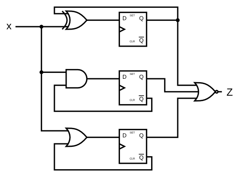
Write your solution here
module top_module (
    input clk,
    input x,
    output z
);
	wire q1,q2,q3;
    initial begin //初始化
        q1 = 0;
        q2 = 0;
        q3 = 0;
    end

    flip_flop inst1(clk,q1^x,q1);
    flip_flop inst2(clk,(~q2)&x,q2);
    flip_flop inst3(clk,(~q3)|x,q3);

    assign z = ~(q1|q2|q3);

endmodule

module flip_flop(
    input clk,
    input d,
    output q
    );
    always@(posedge clk)
        q<=d;
endmodule
Exams/ece241 2013 q7
A JK flip-flop has the below truth table. Implement a JK flip-flop with only a D-type flip-flop and gates. Note: Qold is the output of the D flip-flop before the positive clock edge.
| J | K | Q |
|---|---|---|
| 0 | 0 | Qold |
| 0 | 1 | 0 |
| 1 | 0 | 1 |
| 1 | 1 | ~Qold |
Write your solution here
module top_module (
    input clk,
    input j,
    input k,
    output Q);

    always@(posedge clk)
        case({j,k})
            2'b00:Q<=Q;
            2'b01:Q<=0;
            2'b10:Q<=1;
            2'b11:Q<=~Q;
        endcase
endmodule
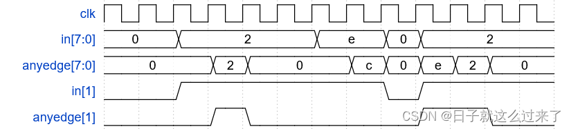
Edgedetec
For each bit in an 8-bit vector, detect when the input signal changes from 0 in one clock cycle to 1 the next (similar to positive edge detection). The output bit should be set the cycle after a 0 to 1 transition occurs.
Here are some examples. For clarity, in[1] and pedge[1] are shown separately.
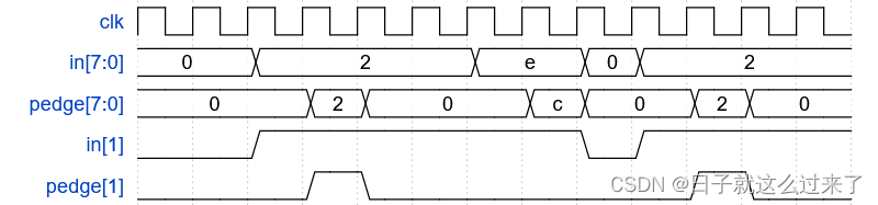
Write your solution here
module top_module (
    input clk,
    input [7:0] in,
    output [7:0] pedge
);
    //这里是想要获取输入信号的上升沿,采用的方式是对输入信号进行打一拍的操作,
    //然后将输入信号与打拍后的信号进行与非就抓取到了输入信号的上升沿。
    reg [7:0] last_in;
    always@(posedge clk) begin//非阻塞赋值:由时钟节拍决定
        last_in <= in;//记住上一个周期的状态  第一个时钟执行右边 第二个时钟赋值
        //需要用到跳变沿的来自同一时钟域的输入,寄存一次即可。
        pedge <= in&(~last_in);
        //第一个时钟执行右边(last_in还未赋值。等待)
        //第二个时钟执行右边(last_in为上一个周期的状态,in为这个周期的状态)
        //第三个时钟赋值
//举例子:in 每个时钟取值 0 2 2
//第一个时钟(0) in 为0 存储到寄存器(0000 0000)
//第二个时钟(2) last_in 从寄存器得值为 0,in&(~last_in)运算得到 2 存储到寄存器中 (0000 0010 & 1111 1111)
//第三个时钟(2) pedage 从寄存器得值为 2 (0000 0010)
    end
    //关于FPGA中“打一拍”的含义,我们可以理解为把某个信号延迟了一个时钟周期,
    //推而广之:“打两拍”就是延迟两个时钟周期,“打n拍”就是延迟n个时钟周期。
    //将信号打一拍的方法是将信号通过一次寄存器

    //非阻塞过程语句的执行不会阻塞下一条语句的执行。仿真过程中在遇到非阻塞型过程赋值语句后,
    //先计算右端赋值表达式的值,然后等到仿真时间结束时再将右侧的值赋给左面。
    //非阻塞赋值先等到普通运算结束后再进行赋值。
	//非阻塞赋值内添加了寄存器,保证了不会立即赋值给寄存器变量,会在下一个时钟变化沿进行赋值

//五条原则:
//1.全局时钟的跳变沿最可靠。
//2.来自异步时钟域的输入需要寄存一次以同步化,再寄存一次以减少亚稳态带来的影响。
//3.不需要用到跳变沿的来自同一时钟域的输入,没有必要对信号进行寄存。
//4.需要用到跳变沿的来自同一时钟域的输入,寄存一次即可。
//5.需要用到跳变沿的来自不同时钟域的输入,需要用到3个触发器,前两个用以同步,
  //第3个触发器的输出和第2个的输出经过逻辑门来判断跳变沿。

/* verilog代码模板
always @ (posedge Clk) //不对输入信号进行寄存
begin
if (inputs)
begin
...
end
...
end
always @ (posedge Clk) //对输入信号寄存一拍
begin
inputs_reg <= inputs;
if (inputs_reg == 1'b0 && inputs == 1'b1)
begin
...
end
...
end
always @ (posedge Clk) //对输入信号寄存三拍
begin
inputs_reg1 <= inputs;
inputs_reg2 <= inputs_reg1;
inputs_reg3 <= inputs_reg2;
if (inputs_reg2 == 1'b1 && inputs_reg3 == 1'b0)
begin
...
end
...
end
*/
endmodule
Edgedetect2
For each bit in an 8-bit vector, detect when the input signal changes from one clock cycle to the next (detect any edge). The output bit should be set the cycle after a 0 to 1 transition occurs.
Here are some examples. For clarity, in[1] and anyedge[1] are shown separately
Write your solution here
module top_module (
    input clk,
    input [7:0] in,
    output [7:0] anyedge
);
    reg [7:0] last_in;
    always@(posedge clk) begin
        last_in <= in;
        anyedge <= (~in) & (last_in) | (in) & (~last_in);
        //(in) & (~last_in)表示任意值(例如:1)变0检测·
        //(~in) & (last_in)表示0变任意值(例如:1)检测
    end


endmodule
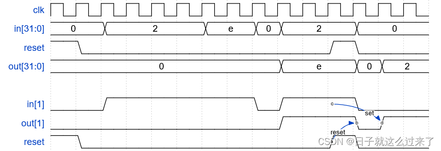
Edgecapture
For each bit in a 32-bit vector, capture when the input signal changes from 1 in one clock cycle to 0 the next. "Capture" means that the output will remain 1 until the register is reset (synchronous reset).
Each output bit behaves like a SR flip-flop: The output bit should be set (to 1) the cycle after a 1 to 0 transition occurs. The output bit should be reset (to 0) at the positive clock edge when reset is high. If both of the above events occur at the same time, reset has precedence. In the last 4 cycles of the example waveform below, the 'reset' event occurs one cycle earlier than the 'set' event, so there is no conflict here.
In the example waveform below, reset, in[1] and out[1] are shown again separately for clarity.
Write your solution here
module top_module(
    input in,
    input [1:0] state,
    output [1:0] next_state,
    output out); //

    parameter A=0, B=1, C=2, D=3;

    // State transition logic: next_state = f(state, in)
    always@(*) begin
        case(state)
            A:if(in)
                  next_state <= B;
              else
                  next_state <= A;
            B:if(in)
                  next_state <= B;
              else
                  next_state <= C;
            C:if(in)
                  next_state <= D;
              else
                  next_state <= A;
            D:if(in)
                  next_state <= B;
              else
                  next_state <= C;
			default:next_state <= next_state;
        endcase
    end

    // Output logic:  out = f(state) for a Moore state machine
    assign out = (state == D)?1:0;


endmodule
Dualedge
You're familiar with flip-flops that are triggered on the positive edge of the clock, or negative edge of the clock. A dual-edge triggered flip-flop is triggered on both edges of the clock. However, FPGAs don't have dual-edge triggered flip-flops, and always @(posedge clk or negedge clk) is not accepted as a legal sensitivity list.
Build a circuit that functionally behaves like a dual-edge triggered flip-flop:
(Note: It's not necessarily perfectly equivalent: The output of flip-flops have no glitches, but a larger combinational circuit that emulates this behaviour might. But we'll ignore this detail here.)
Write your solution here
module top_module (
    input clk,
    input d,
    output q
);
    wire q1,q2;
    always@(posedge clk) begin
        q1 <= d^q2;
    end
    always@(negedge clk) begin
        q2 <= d^q1;
    end
    assign q = q1^q2;
endmodule


 被折叠的 条评论
为什么被折叠?
被折叠的 条评论
为什么被折叠?
 到【灌水乐园】发言


