


目录
嵌入式系统概念
嵌入式系统(Embedded system):
- 是为执行特定任务而设计的计算机系统
- 通常被嵌入在系统或设备中,而不是计算机中
例子1:路由器(network router)
It is a computing system dedicated to the task of routing packets in a network.
It is a standalone embedded system
它是一个专门用于网络中分组路由任务的计算系统。
它是一个独立的嵌入式系统
例子2 微波炉(microwave oven)
it is an electronic appliance which happens to contain a computing system to control its user interface and cooking time
The embedded system is the user interface/cooking controller
It is embedded within the microwave oven appliance
是一种电子电器,碰巧包含一个计算机系统来控制它的用户界面和烹饪时间
嵌入式系统是用户界面/烹饪控制器
它嵌入在微波炉电器中
嵌入式系统的主要组成:(具体之后详细讲)
- Input/output
-
- to communicate with sensors, actuators, displays etc. (与传感器、执行器、显示器等进行通信)
- Processor(处理器)
-
- the computing engine (计算引擎)
- [Optional] Hardware acceleration (邮件加速器)
-
- E.g. ASICs, FPGAs, AI accelerators, etc
- Firmware (固件)
-
- embedded software
嵌入式系统在哪些方面与其他电脑系统不同?
- Task specific, not general purpose 特定用途
- real time 实时
it has deadlines for system response to an input 有系统响应输入的截止日期
Outputs must be both correct and on time
Predictable vs. fast - fault handling 故障处理
- power and operating environment 电源和操作环境
- cost 成本
- range of processor types 处理器种类
4, 8, 16, 32 bit
About 98% of all 32-bit processors are used in embedded systems, not PCs. - Resource constrained 资源限制
例子: PIC16F876A has just 368 Bytes of data memory
Often few input buttons and simple displays. Greatly affects software design.
只有少量输入和简单显示,影响软件设计。 - Program code in ROM
Affects data initialization, debugging. 影响数据初始化和调试
ps: ROM(只读内存(Read-Only Memory)简称)。ROM所存数据,一般是装入整机前事先写好的,整机工作过程中只能读出,而不像随机存储器那样能快速地、方便地加以改写。 - Specialized development/debugging tools 专门的开发调试工具
Cross compiler/assembler 交叉编译器/汇编器
Emulator 模拟器
In-Circuit Debugger 电路内置调试器
Processor Technology 处理器技术
三种处理器 processor
- GPP
General Purpose Processor 通用处理器
Programmable for any application
Usually requires external support hardwar
可为任何应用编程,通常需要外部支持 - ASIP
Application Specific Instruction Processor 特定应用指令处理器
Optimized for specific application areas, but still software programmable
针对特定的应用领域进行优化,但仍可通过软件进行编程 - SPP
Single purpose processor 单用途处理器
Optimized for one specific task only with no flexibility.
Algorithm “hard coded” in finite state machine, not software programmable.
只针对一个特定的任务进行优化,没有灵活性。
算法“硬编码”在有限状态机中,不是软件可编程的。
处理器指令集
ISC(复杂指令集计算)例如 Intel x86 family
- The main goal is to complete a task with as few instructions as possible
主要目标是用尽可能少的指令完成一项任务。 - 处理器硬件更为复杂,每条指令可能有一系列底层操作(underlying operations)
RISC(精简指令集计算)例如:ARM Advanced RISC Machine
- The focus is on really simple instructions that can be executed in one instruction cycle
重点是可以在一个指令周期内执行的非常简单的指令 - 硬件被简化,编译器承担更多的工作
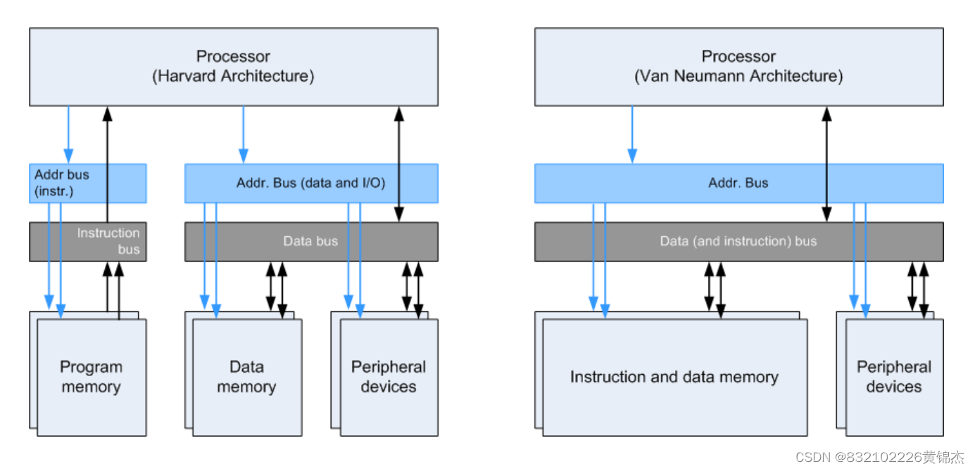
Memory architecture 内存架构
| 体系结构 | 结构 | 特点 |
|---|---|---|
| 冯·诺依曼 | 程序和数据共用一个存储空间;采用单一的地址及数据总线。 | 执行指令时, 先从储存器中取指解码,再取操作数执行运算,即使单条指令也要耗费几个甚至几十个周期,在高速运算时,在传输通道上会出现瓶颈效应。 |
| 哈佛 | 程序和数据存储在不同的存储空间中,每个存储器独立编址、独立访问。 | 分离的程序总线和数据总线可允许在一个机器周期内同时获取指令字(来自程序存储器)和操作数(来自数据存储器),从而提高执行速度,提高数据的吞吐率。因此取指和执行能完全重叠,具有较高的执行效率。 |
在给定的时钟速度下,如果没有内存缓存(典型的低端处理器),哈佛架构将允许更快的执行,因为指令和数据可以同时读取
总线 bus
字长(word size),是CPU一次能处理的二进制数的位数
位宽(bit wide),就是内存或显存一次能传输的数据量
数据总线 data bus 单位:bit,D
(1) 是CPU与内存或其他器件之间的数据传送的通道。
(2)数据总线的宽度决定了CPU和外界的数据传送速度。
(3)每条传输线一次只能传输1位二进制数据。eg: 8根数据线一次可传送一个8位二进制数据(即一个字节)。
(4)数据总线是数据线数量之和。
地址总线 address bus 单位:bit,A
(1)CPU是通过地址总线来指定存储单元的。
(2)地址总线决定了cpu所能访问的最大内存空间的大小。eg: 10根地址线能访问的最大的内存为1024位二进制数据(1024个内存单元)(1B)
(3)地址总线是地址线数量之和。
控制总线
(1)CPU通过控制总线对外部器件进行控制。
(2)控制总线的宽度决定了CPU对外部器件的控制能力。
(3)控制总线是控制线数量之和。
总结:
地址总线的宽度决定CPU的寻址能力;
数据总线的宽度决定CPU与其他元器件一次最大传送的数据量;
控制总线决定CPU对其他元器件的控制能力。
与嵌入式相关
- D determines the native integer size which determines the kind of arithmetic that
can be done with single instructions
D确定了本机整数的大小,该大小决定了可以用单个指令完成的算术类型 - A determines the max addressable memory
A确定了最大可寻址内存
Opcode 操作码
Instruction processing and pipelining 指令处理和流水线
Instruction cycles vs. Clock Cycles
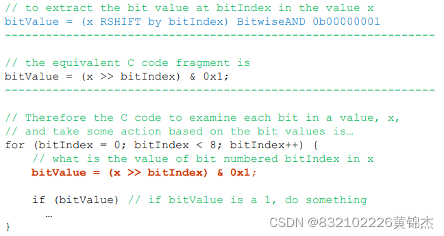
位操作符
a&b 将a和b转为二进制后进行“与”操作
| “或”
^ 异或 00=0 10=1 01=1 11=0
a<<n 转为二进制后整体向左移动n位,然后用0填满
a<<n 数学算法= a*2n
a>>n 右移n位,正数用0,负数用1,填满
a>>n 数学算法= a/2n
(左乘右除)
a>>n 右移n位,都用0填满
~a 把a二进制的0和1互换
~a 数学算法=(-a)-1
I/O synchronization
管理输入/输出发生的时间和方式称为I/O同步
polling I/O 轮询
定时对各种设备轮流询问一遍有无处理要求。轮流询问之后,有要求的,则加以处理。在处理I/O设备的要求之后,处理机返回继续工作。
the software “polls” (checks) the device to see if an I/O operation is possible/required
◼ For simple I/O operations, polling may only be required to check the current “value” or “flag bits” in a device register
◼ More complex I/O may consist of initiating some I/O and then polling until it has been completed
不同的轮询操作
仅轮询一次 Poll once and forget
◼ In this case, we don’t wait or check for completion – once initiated, we assume it will complete quickly enough. E.g. Digital port input/output 数字端口输入/输出
◼ Other work can continue immediately.
小结:这种轮询操作很快就会完成,其他工作可以立即继续
轮询阻塞 Busy wait polling (blocking)
◼ Wait for operation to complete, checking (polling) constantly. E.g.waiting for ADC conversion complete once initiated.
◼ No other work can be done while we wait
小结:这种轮询操作需要等待ADC转换完成,等待期间没有别的工作进行
多任务轮询 Multi-task polling (non-blocking)
◼ Other work can proceed while waiting for operation to complete
◼ check back (poll) at regular intervals to detect I/O operation completion
小结:这种轮询操作进行时其他操作可以同时进行,定期轮询来检查I/O
轮询优缺点
Advantages
Simple to implement 易于实现
I/O is synchronous, taking place in the application foreground. IO同步
Device priority is easy to change.优先级易于改变
- Determined by the order in which software polls (checks) the devices.
- Device priority is used to decide what to handle first when several I/O devices need servicing at the same time
Disadvantages
CPU time may be wasted continually polling. 持续轮询浪费CPU时间
Response time/throughput is often a compromise
Not best choice when I/O takes place infrequently or at unpredictable intervals
IO同步问题
- The CPU/app is faster than the I/O device
解决方法:
- The app needs to buffer output data so that it can be written at the slower device rate over the course of multiple superloops.
通过缓冲(buffer)输出数据来以较慢的速度写入设备。 - The app can do other work while not servicing the IO device.
app/CPU可以做一些其他工作
- The I/O device is (temporarily) faster than the CPU/app
This only works if the fast IO device is only active in short bursts of activity. IO设备短时间爆发活动
- The app needs to buffer input data that is arriving quickly without doing any substantial processing work.
app缓存快速到达的输入数据,先不进行处理 - The app must respond to device input with low latency (delay between stimulus and response) to avoid missing data
app以低延迟(刺激和响应之间的延迟)响应输入,以免丢失数据 - Later when the input burst has ended, the app can process the buffered data
等输入爆发结束后再处理缓冲的数据
- The I/O device needs or supplies data at regular, predictable times. IO设备需要定期提供数据
- Poll at regular intervals corresponding to the predictable IO times
按可预测的IO时间间隔进行轮询
- The I/O device needs or supplies data at irregular, unpredictable times.IO设备需要不定期提供数据
- Poll at regular intervals corresponding to the minimum latency required to handle the irregular IO times. E.g. a 10 ms minimum latency on unpredictable button presses requires polling at 10 ms (or smaller) intervals.
根据不规则IO时间的最小延迟来进行定期轮询
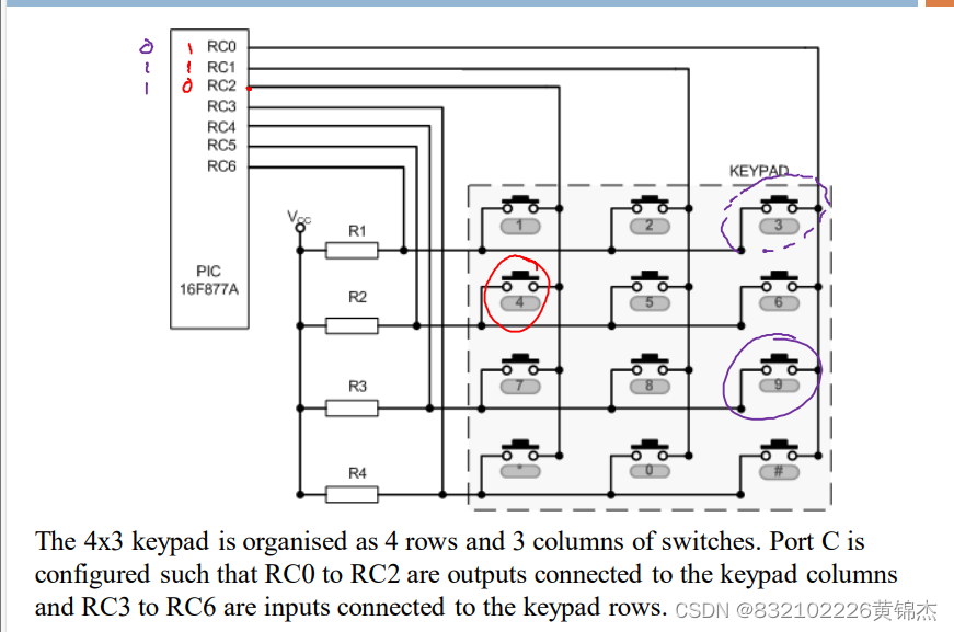
Digital Port Input/Output
基本数字I/O设备包括:
Switch (input) 开关
Simple keypad (e.g. 3 x 4 phone keypad, input) 简单键盘
LED (output)
7 segment display (output) 段码显示板
Speaker/beeper (output) 蜂鸣器
I/O端口的架构
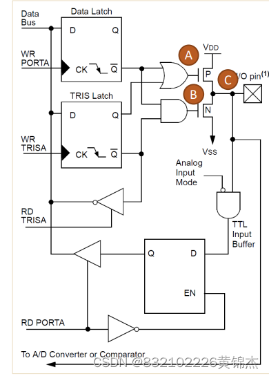
Input port comprises
- Buffer: isolate input latch from input current source
缓冲:将输入锁存器与输入电流源隔离 - Input latch: to briefly hold (*) the current value on the latch output (connected to the data bus) so that the CPU can read it.
输入锁存器:短暂地保持锁存器输出(连接到数据总线)上的当前值,以便CPU可以读取它。
Output port comprises
- Output latch: briefly enabled (*) so that CPU can set output level via the data bus; then disabled so that output is held stable at that value (while data bus reused for next instruction)
输出锁存器:短暂启用,以便CPU可以通过数据总线设置输出级别;然后禁用,以便输出稳定在该值(而数据总线可用于下一条指令)
Bidirectional port 双向端口 - Contains additional latch and logic to enable just one of the input or output directions
包含额外的锁存器和逻辑,仅启用一个输入或输出方向
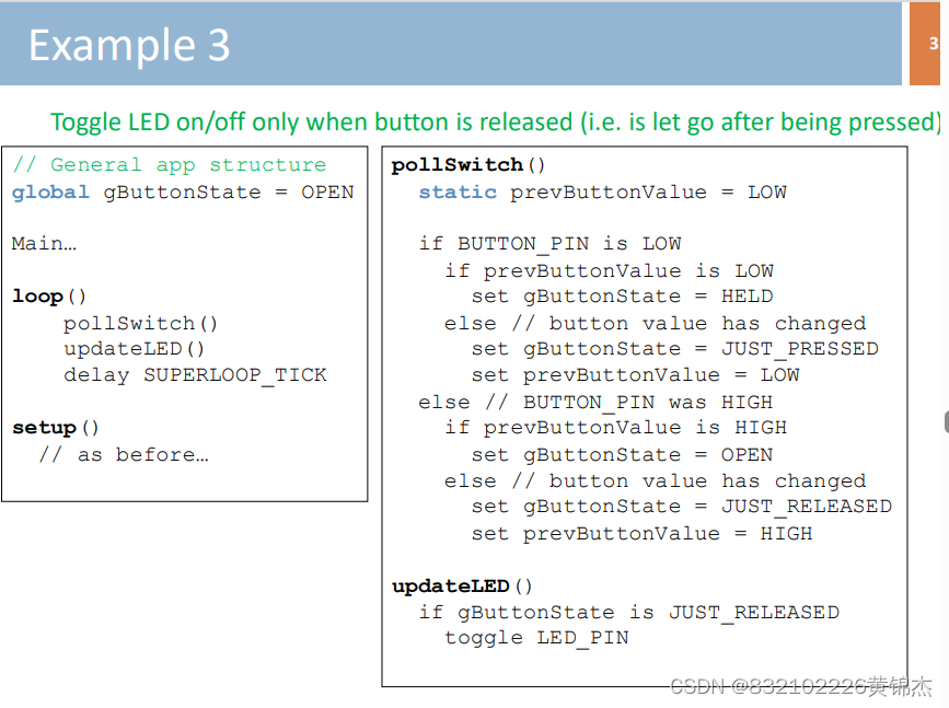
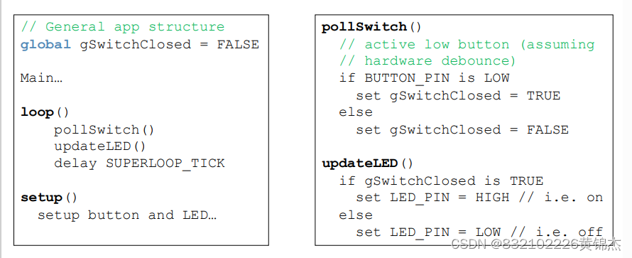
Example
下面是一些专注于数字端口I/O的简单轮询示例
为了简单起见,我们假设一个按钮开关连接到输入引脚,一个LED连接到输出引脚
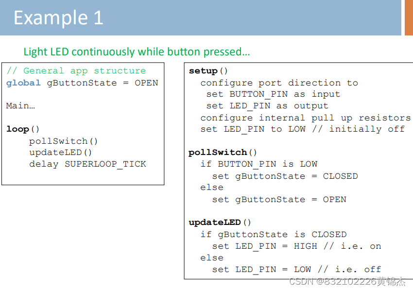
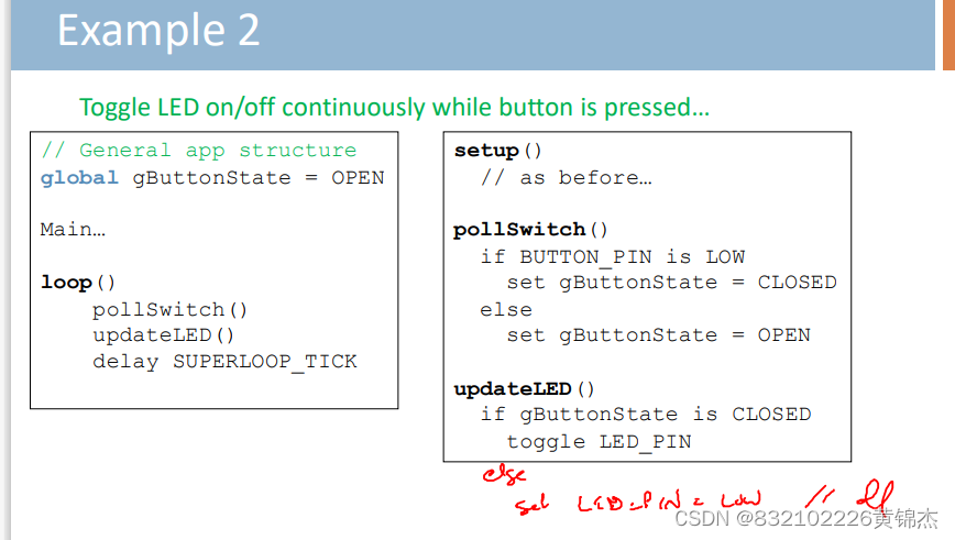
ps:toggle 切换
* Switch debounce 开关防反跳
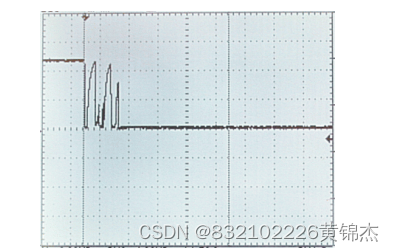
未反弹开关产生的电压
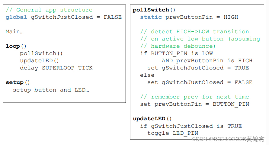
Common/useful polling patterns 常见轮询模式
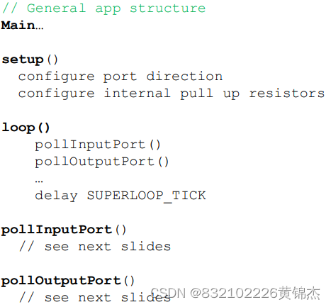
通用I/O端口伪代码
模式1:轮询以检测瞬时状态,连续行动
按钮电压改变就进行操作
模式2:轮询以检测特定的更改,仅在特定的更改发生时执行一次操作
仅在按钮按下的时候执行操作
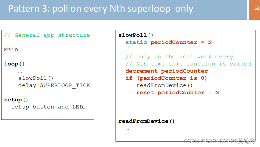
模式3:只对第n个超级循环进行轮询
题目:
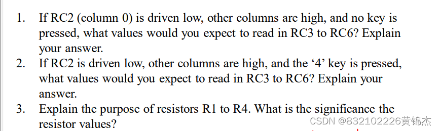
(i)
- 预期值:RC3 到 RC6 所有输入引脚上的高 (逻辑 1)。
当 RC2 被拉低时,它会在连接到行 4、3 和 2 的各自电阻 R4、R2 和 R1 之间产生电位差。但是,由于没有按下任何键,这些电阻将充当开路,防止电流流向输入引脚。
没有电流流动,输入引脚 RC3 到 RC6 保持其高阻状态,通常被 MCU 解释为高 (逻辑 1) 值。
(ii)
- 预期值:RC3、RC4 和 RC6 上的高 (逻辑 1);RC5 上的低 (逻辑 0)。
当按下“4”键时,它将通过 S4 完成一个电路。
这允许电流从 RC2 (被拉低) 通过 S4 流到 RC5 (输入引脚),将 RC5 拉低 (逻辑 0)。
其他输入引脚 RC3、RC4 和 RC6 保持高 (逻辑 1),因为由于没有在这些行中按下任何键,它们各自的电阻 (R3、R2 和 R1) 仍然充当开路。
(iii)
电阻 R1 到 R4 的目的:
**上拉电阻:**它们确保在没有按下任何键时,输入引脚 RC3 到 RC6 保持在定义的高状态 (逻辑 1)。这可以防止它们漂浮并拾取杂散信号。
**电流限制:**它们限制按下按键时电流流动,保护键盘和 MCU 输入引脚免受潜在损坏。
100 kΩ 电阻值的重要性:
**高阻值:**100 kΩ 的相对高值可最小化电流消耗,同时仍为输入引脚提供足够的上拉强度。这有助于节省电力并降低电路总电流。
**上拉强度和电流限制之间的平衡:**该值在提供足够的上拉以确保可靠的输入读数和将电流限制在键盘和 MCU 的安全水平之间取得平衡。
Analogue I/O 模拟IO
Analogue I/O typically applies to
- Signals from sensors (temperature, pressure,acceleration, etc) 传感器信号
- Signals to drive actuators (motors, etc.) 驱动器信号
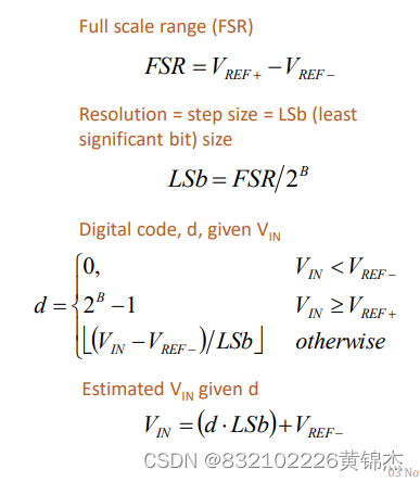
ADC
- 将模拟输入的电压转换为数字表示
- 采集时间(Acquisition time)和转换时间( conversion time)将决定最大采样率(sample rate)
- 如果没有外部参考电压,Vref-=Vss,Vre+=Vdd
-
- VDD:D=device,表示器件的意思,即器件内部的工作电压。
-
- VSS:S=series,表示公共连接的意思,通常指电路公共接地端电压。
- 创建外部参考电压(external voltage)的方法是使用电阻分压器电路(resistor divider circuit)
- ADC将电压分为大小相等的步长(steps)
- B个比特,则step=(Vref+ - Vref- / 2^B)
常见计算
采样率 fs=2*fmax
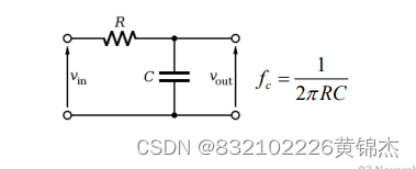
为了防止 aliasing 需要使用滤波器去除大于2fs的信号
Comparator 比较器
1表示VIN+在VIN-之上,0表示在VIN-之下
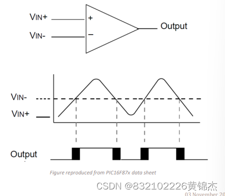
为了防止参考水平附近的振荡,基本的解决方案是使用两个阈值(thresholds)实现滞后:低阈值和高阈值
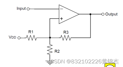
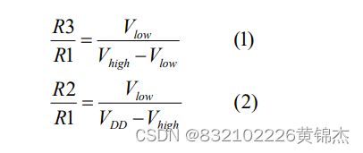
The result is that R2 and R3 can both be expressed as a multiple of R1.
EXAMPLE: VDD=5V, desired high threshold Vhigh = 2.7V and low threshold Vlow = 2.3V. Sub into equation 1 and 2 yields R3 = 5.75 * R1 and R2 = 1 * R1. If we choose R1 = 100 kΩ then R2 = 100 kΩ and R3 = 575 kΩ
异步串行通信 Asynchronous Serial Communications
串行通信
在一条传输线上,数据以“位”为单位进行逐个传输,即为串行通信
- 异步串行通信,是指发送方与接收方,使用各自的时钟控制数据发送和接收过程(为使双方收发协调,要求双方时钟尽可能一致);
- 同步串行通信,则是发送方时钟直接控制接收方时钟,使双方完全同步(同步方法有“外同步和自同步”两种)。
串行(Serial)相对于并行(parallel)通信的优点:
Parallel cables can be bulky and expensive.并行的电缆庞大昂贵
Serial communication requires fewer wire.较少的电线
Serial data can be transmitted over longer distances.可以传输更长的距离
串行接口:FireWire, USB, PCI Express
异步串行的连接方式:
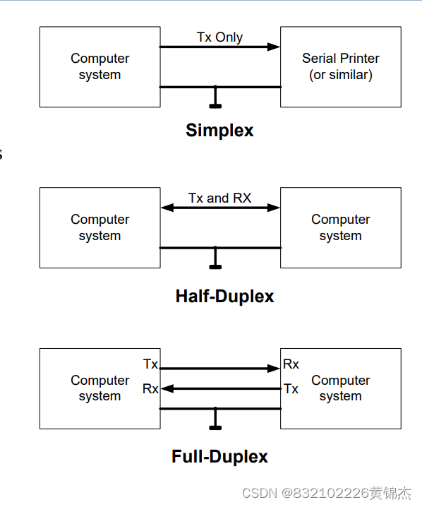
- Simplex 单工:数据仅能沿一个方向传输,不能实现反向传输(只能A→B,不能B→A)
- Half-Duplex 半双工:数据可以沿两个方向传输,但同一时刻,只能接收或者发送
- Full-Duplex 全双工:数据可以沿两个方向传输,且可以同时进行
异步串行属性
- 异步串行通信用于发送/接收串行数据,而无需显式同步(without explicitly synchronising)发射器和接收器的时钟
- 接收器必须同步仅使用发射信号和一些事先同意/配置的时间
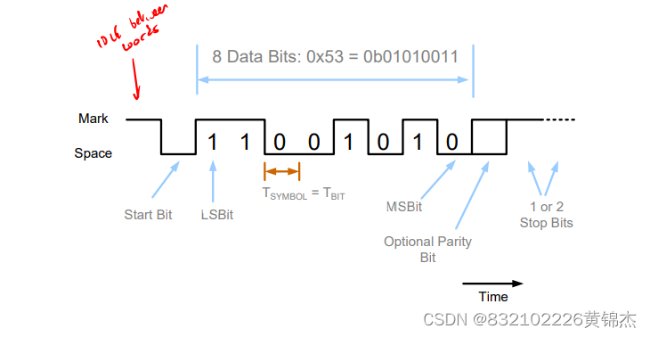
- 数据每次发送一个字节,每个字节被封装(packaged)在一个异步字( asynchronous word)中,其中包括启动/停止位(overhead)以帮助同步
- 每个异步字asynchronous word (data+overhead)中的比特位映射到顺序(串行)传输的符号。
- 符号发送/接收的速率称为符号速率或波特率(例如9600baud)。Symbol rate or Baud rate
- 异步串行通信是点对点的,通常是全双工(即分开的发送和接收线路),但也可以使用半双工和单工
数据格式
- 起始位 start bit
起始位为0。
- 通讯线在空闲状态时保持高电平,因此出现下降沿即可判定为数据传输开始;
- 另外,由于数据位定长,且起始位在一次接收中只判定一次,所以不用担心数据位中的0误识别成起始位。
- 数据位
- 数据位可以是5/6/7/8位,传输时低位在前、高位在后。
- 要传输的8位数据,最低有效位(LSb)优先
- 奇偶校验位 parity bit
校验位可以省略,当需要使用校验位时:
- 奇偶校验位为1或0;
- 奇校验时,数据位、校验位中1的个数,应该是奇数;
- 偶校验时,数据位、校验位中1的个数,应该是偶数。
- 停止位 stop bits
停止位为1。
- 停止位可以是1位的长度、1.5位的长度、2位的长度(位数的本质含义是信号出现的时间,故可有分数位);
- 两个停止位可以让接收方在下一个异步字到达之前有更多的时间来处理接收到的数据
- 另外,由于数据位定长,所以停止位位置固定可知,接收时只需判定停止位是否为1即可。
在异步串行中,仅使用两个电压电平,因此字母表大小为2,因此每个符号的位数为1
- 这两个符号是电压等级,称为:mark(高) space(低)
- 符号周期为 1/symbolrate
波特率=符号速率=每秒符号数
Effective data rate=bit rate*data bits per asyncword / totalbits per asyncword
maximum rate
= 总的位数乘符号周期
specification规范
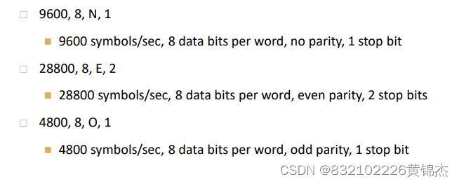
一般使用:baudRate, numDataBitsPerWord, parity, numStopBits 来指定一个异步串行通信
例子:
bit banging
从MCU实现异步串行通信的技术叫做“bit banging”,在这个技术中:
- Tx和Rx通信线路直接连接到数字I/O端口
- 单片机驱动Tx线的高和低在正确的时间发送一个格式良好的异步字
- MCU必须检查(轮询)Rx行以定期间隔检测开始位,因此存在异步字的后续位
例子:该程序运行时每秒发送一个原点
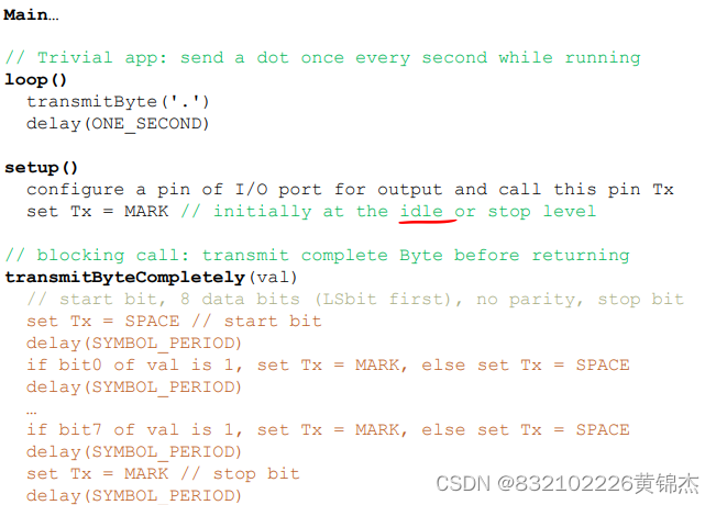
transmit(val) 配置异步串行的各个位(bit)起始位0,数据位根据val来,停止位1,中间间隔时间为symbol 周期
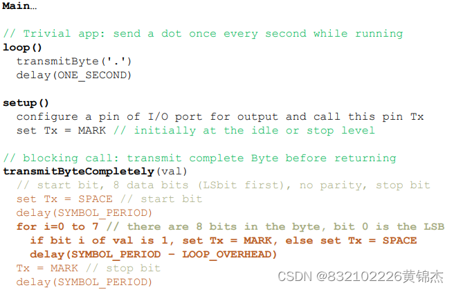
中间位改为for循环填写
通用异步接收发送(UART)设备
The Universal Asynchronous Receive Transmit (UART) device
用于异步串行通信的专用辅助设备
Tx:将并行数据转换为串行比特流
Rx:将串行比特流转换为并行数据。
控制与其他uart之间的握手信号
处理传输和接收数据的位定时。
提供与CPU的接口信号。
UART的数据通信
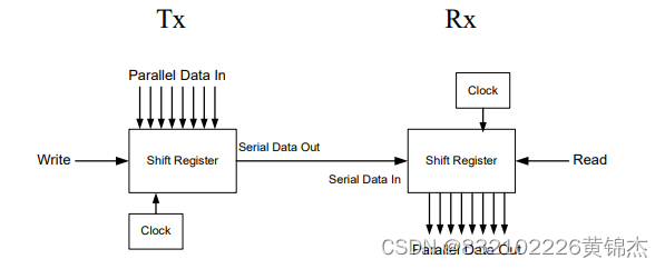
- Tx: Parallel to serial
- Rx: serial to parallel
- A full duplex UART has both Tx and Rx parts
Tx figures explained
TXREG是程序写入要传输的数据的地方
TSR(传输移位寄存器)是数据被复制到导线上移位的地方。这意味着当您将下一个单词写入TXREG时,一个单词可能在TSR中“in progress”。这在时序图中显示为在word 1之后将word 2复制到TXREG。
TXIF(传输中断标志)仅在TXREG为空时设置(1)(不是在一个字已经完全传输时),并且它只能通过加载TXREG的值来claer(到0)。
仅当TSR为空时(即数据已传输完毕),TRMT位为1。如果TSR当前正在传输一个单词,则TRMT是clear(0)。
TX9D是第9位数据位,允许软件校验实现。这是可选的。
SPEN启用UART发送器-如果clear,没有任何东西可以发送。
集成电路(I2C) 和 串行外设接口(SPI)
EEPROM(带电可擦可编程只读存储器)是用户可更改的只读存储器(ROM),其可通过高于普通电压的作用来擦除和重编程(重写)。
两种同步通信协议:
Inter Integrated Circuit
The Serial Peripheral Interface
他们通常用于连接微控制器到外设
比如:: PIC microcontroller to ADC, or DAC, or EEPROM, or USB interface, or Bluetooth Radio
他们的共同点
使用控制器/外设架构
控制器和外设通过总线连接
一个专用时钟信号(SCL)传输独立于数据
数据首先传输MSb(最高有效位)
I2C的特性(与SPI不同之处):
- I2C总线组成有: erial data (SDA) and serial clock (SCL) 串行数据(SDA)和串行时钟(SCL)
- 只有一条数据线,通信为半双工的(half-duplex),即控制器和外设(Controller and Peripheral)不能同时传输
- SDA和SCL线路使用上拉电阻(pull up resistors)和“float high ”
- 设备根据需要拉低SDA和SCL线路
- 控制器通常控制SCL,但外围设备可以拉低SCL暂停传输(这称为时钟拉伸clock stretching)
I2C协议(与SPI不同之处)
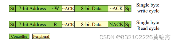
将所有通信分为两种操作:读(控制器向外设请求数据)和写(控制器向外设发送数据)。
接收方必须确认收到的所有数据(ACK或NAK),这有助于通信的健壮性
控制器传输一个I2C地址作为任何读/写操作的第一部分,以选择与哪一个总线连接的设备(可能有许多)通信
协议比SPI更复杂(稍后见
I2C
编码原理
- I2C传输一个7位或10位寻址方案来选择设备。
- 仅当SCL为低时,transmitter (Controller or Peripheral)发送器仅改变SDA的电平(level)
- 当SCL为高时,receiver (Peripheral or Controller)接收器读取相应的位值
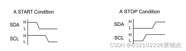
start and stop conditions
- 在空闲状态(idle state)SCL和SDA为高平
- Start (SDA low后跟SCL low)保留I2C总线并发出数据传输开始的信号
- Stop (SCL high后跟SDA high)表示数据传输结束并释放总线
SPI
timer
(source) Clock
定时器通常可以配置为使用一个不同的时钟源为其底层定时输入,例如PIC允许指令时钟,外部时钟等。
Tick
定时器/计数器的值在每个时标上递增1。
Pre-scaler
位于源时钟信号和定时器之间。
分频器值N意味着每N个时钟周期发生一个时钟时标,而不是每个时钟周期
Post-scaler
后缩放器位于定时器重置和定时器事件信号功能之间
后标量值M,意味着计时器事件只会在计时器重置M次后才会发出信号,而不是每次重置
Prescaler前分频器
计时器通过每个时标增加或减少计数寄存一次来标记时间
如果没有分频器(或分频因子prescaling factor为1:1或1x),则源时钟信号的每个时钟周期有一个时标
如果使用的分频器的因子大于1x,那么时钟不是发生在每个源时钟周期上,而是发生在时钟周期的指定倍数上。例如,1:4或4x意味着每4个源时钟周期有一个时钟周期
分频器允许计时器(通常有一个有限的计数器)测量较长的持续时间(durations)
Postscaler后分频器
正常情况下,当定时器达到特定值时,会发生定时器事件
当没有后分频器或后分频因子(postscaling factor)为1x时,定时器事件直接导致超时信号或中断(timeout signal or interrupt)
当后缩放因子大于1x时,则在发出超时或中断信号之前,必须发生指定数量的定时器事件,例如,8x意味着在发出超时信号之前必须发生8个定时器事件
像预调度器一样,后调度器允许计时器(通常有一个有限的计数器)测量较长的持续时间
Timer events, timeouts, and interrupts
当定时器计数器达到配置值或定时器计数器寄存器滚动时,定时器事件发生(例如,8位定时器寄存器从0xFF滚动到0x00)。
- 我们使用的是配置值还是滚动,通常取决于特定的定时器
定时器事件发生时
- 它可以被配置为自动重置定时器,这允许定时器以固定的周期生成事件
- 如果没有后缩放器或后缩放因子为1,则立即生成超时。
否则,超时仅在M个定时器事件之后产生,其中M是后缩放因子。
当超时发生时,根据定时器的不同,可以将其配置为
- 生成中断——允许程序立即采取行动(对实时很重要)
- 产生一个数字信号,可以在内部外设(微控制器上)或外部外设上启动某些动作
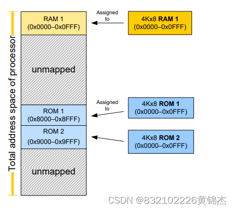
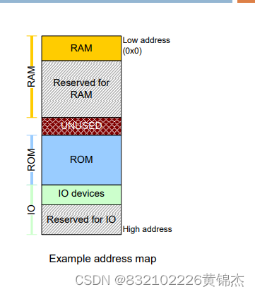
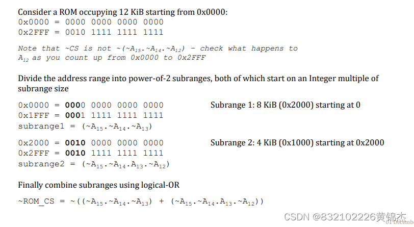
adress map
最小地址在顶部,最大地址在底部
最大地址为2^k
k是地址行数
reserved:映射


 7998
7998


 被折叠的 条评论
为什么被折叠?
被折叠的 条评论
为什么被折叠?
 到【灌水乐园】发言


