


目录
在linux下获取屏幕的DPCD以及edid信息工具丰富。而windows下就难多了,尤其DPCD。
eDP 链路设计
带开关的eDP链路设计
CBTL06DP212 典型应用在需要选择两个GPU DisplayPort源之一以连接至DisplayPort接收器件或接口的主板上。控制器芯片会通过将选择信号设为HIGH或LOW来选择要使用的路径。由于信号路径的双向性质,CBTL06DP212还可使用在反向拓扑中,例如,将一个显示源器件连接至两个显示接收器件或接口之一
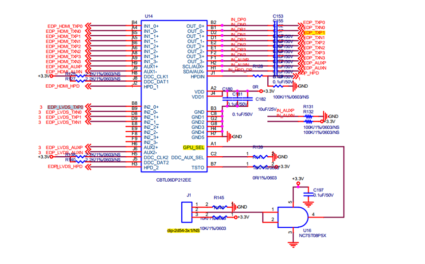
本例上图使用从CPU出一组EDP口(右侧)转换为左侧的一组EDP加一组HDMI
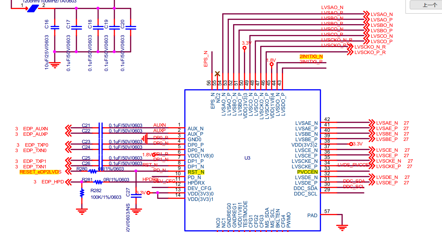
左侧出来的EDP再通过下图转换为LVDS。
注意: 这里辅助通道上有一组选焊的1M电阻。

不带开关的eDP链路设计
这里一个主要差异是 辅助通道上没有一组选焊的1M电阻。
屏检测
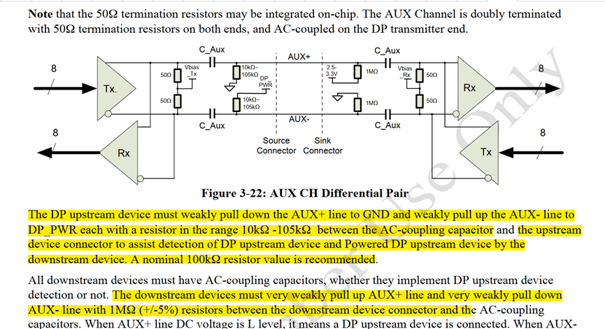
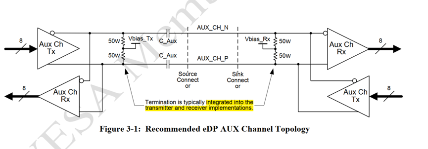
来看规范里面辅助通道的设计,edp与dp的差异。通过下面两个章节可以看到DP在设计上有电阻,主要检测屏与控制器的连接。而edp作为内嵌屏,不热插拔,故而规范里面也就无此设计了。
dp
Page 352页
edp
Windows工具
EDID获取
https://www.entechtaiwan.com/util/moninfo.shtm
MonInfo
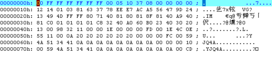
可以获取当前系统的EDID信息,并保存为二进制文件。用于烧到eeprom中。

EDID文件信息
128个字节,直接烧写到EEPROM中,即可。1600x1200的分辨率
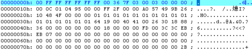
1024x768
EDID 解析及查看工具
时序修改配置
http://www.tinyvga.com/vga-timing
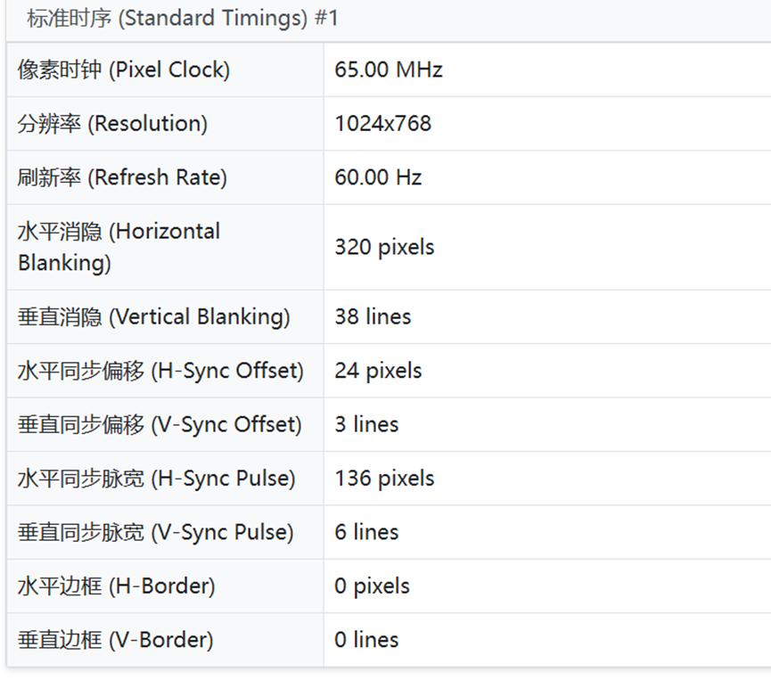
常见时序
一些时序参数可以参考:
Windows驱动参数
安装目录有inf文件。
DisplayFeatureControl”项值确认为“0x000003c7”
\HKEY_LOCAL_MACHINE\SYSTEM\ControlSet001\Control\Class\{4d36e968-e325-11ce-bfc1-08002be10318}\0001”为“0x000003c7”
这个参数修改可能会解决些闪屏问题
linux下解析
在没有焊接EDID的eeprom时,此处xranr查询到为多个显示分辨率。而焊接eeprom后只显示如下一个了。
xrandr
Screen 0: minimum 320 x 200, current 1024 x 768, maximum 16384 x 16384
eDP-1 connected primary 1024x768+0+0 (normal left inverted right x axis y axis) 0mm x 0mm
1024x768 60.00*+
DP-1 disconnected (normal left inverted right x axis y axis)
HDMI-1 disconnected (normal left inverted right x axis y axis)
x86的I2C控制器使能
默认的I2C控制器如下:

 i2cdetect -l

i2c-3         i2c            i915 gmbus dpd                  I2C adapter

i2c-1         i2c            i915 gmbus dpc                  I2C adapter

i2c-4         i2c            AUX A/DDI A/PHY A               I2C adapter

i2c-2         i2c            i915 gmbus dpb                  I2C adapter

i2c-0         smbus         SMBus I801 adapter at 5040           SMBus adapter

i2c-5         i2c            AUX B/DDI B/PHY B               I2C adapter
X86需要在BIOS中使能I2C0控制器。默认关闭了,打开后可以看到多了一个I2C控制器。
i2cdetect -l

i2c-3         i2c            i915 gmbus dpb                  I2C adapter

i2c-1         i2c            Synopsys DesignWare I2C adapter     I2C adapter(此处为I20的控制器)

i2c-6         i2c            AUX B/DDI B/PHY B               I2C adapter

i2c-4         i2c            i915 gmbus dpd                  I2C adapter

i2c-2         i2c            i915 gmbus dpc                  I2C adapter

i2c-0         smbus         SMBus I801 adapter at 5040           SMBus adapter

i2c-5         i2c            AUX A/DDI A/PHY A               I2C adapter

 i2cdetect -y -r 1

     0  1  2  3  4  5  6  7  8  9  a  b  c  d  e  f

00:          -- -- -- -- -- -- -- -- -- -- -- -- --

10: -- -- -- -- -- -- -- -- -- -- -- -- -- -- -- --

20: 20 -- -- -- -- -- -- -- -- -- -- -- -- -- -- --

30: -- -- -- -- -- -- -- -- -- -- -- -- -- -- -- --

40: -- -- -- -- -- -- -- -- -- -- -- -- -- -- -- --

50: -- -- -- -- -- -- -- -- -- -- -- -- -- -- -- --

60: -- -- -- -- -- -- -- -- -- -- -- -- -- -- -- --

70: -- -- -- -- -- -- -- --
VBT的配置
intel_vbt_decode /sys/kernel/debug/dri/0/i915_vbt
BDB block 27 - eDP block:
Panel 14 *
Power Sequence: T3 2000 T7 10 T9 2000 T10 500 T12 5000
Panel color depth: 18 bpp
eDP sDRRS MSA Delay: Lane 1
Fast link params:
rate: 1.62G
lanes: x2 mode
pre-emphasis: none
vswing: 0.4V
Stereo 3D feature: no
T3 optimization: yes
Vswing/preemphasis table selection: Low power (200 mV)
Fast link training: no
DPCD 600h write required: no
PWM delays:
PWM on to backlight enable: 0
Backlight disable to PWM off: 0
Full link params provided: no
Full link params:
pre-emphasis: none
vswing: 0.4V
FAST LINK 与full link
source与sink 支持要求
The eDP device (Source and Sink) must be capable of supporting full link training. Fast link training is mandatory on the Sink, and is an implementation option on the Source
即我们CPU作为source端不是必须实现fast link的。这就是上述VBT中没有被配置fast 为yes的原因。当然我们在其他项目中可以配置此项为yes,然后配置相关swing和预加重参数
fast link定义
Fast Link Training only (training without using AUX transactions).
即不需要辅助通道握手,直接根据配置的参数training。
When DP Source device is resuming the transmission (e.g. after waking from sleep), the Source device may skip the AUX CH handshake for the link training if the following conditions are met:
The Source device has determined that the HPD signal has remained asserted continuously (apart from IRQ_HPD notifications) since the link was last in full operation.
The Source device has read 1 in NO_AUX_HANDSHAKE_LINK_TRAINING bit of DPCD (Bit 6 of Address 3h) after the initial Sink device detection.
故障及解决
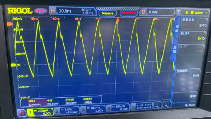
故障时机: 在熄屏,即lvds数据时钟都没有了后,再次重新显示时。
正常时,时钟为65M,而异常时则如下为52M .通过修改上述VBT中fast link为YES 即可解决。
参考资料
https://community.nxp.com/t5/Other-NXP-Products-Knowledge/PTN3460-PTN3460I-FAQs/ta-p/1166765


 476
476

 被折叠的 条评论
为什么被折叠?
被折叠的 条评论
为什么被折叠?
 到【灌水乐园】发言


