


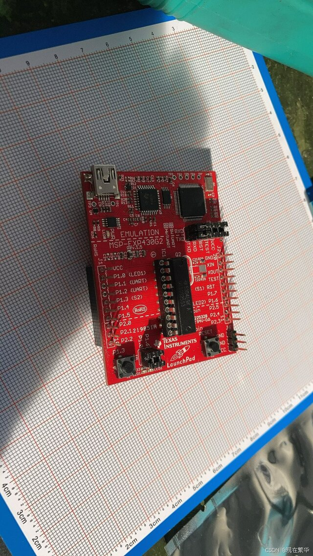
搞了一个msp430g2的开发板,
纸盒装的
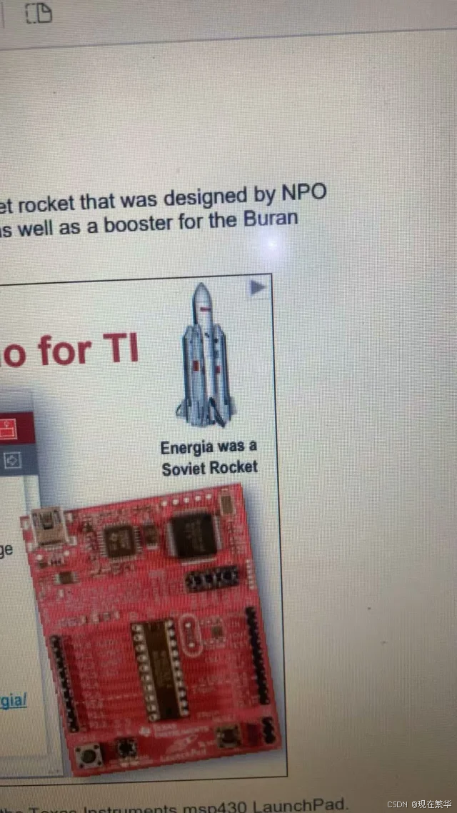
开发板又叫 lunch pad,红色板子,印有火箭logo,入门ide是energia
官方说是某暴风雪-能源号。。
是德州仪器官方的,原板自带pdip-20的芯片,
有一些没有盒子的版本,排针是普通的单侧排针,那种是假货。。
假货并不会便宜超过十块钱,所以完全没必要的。
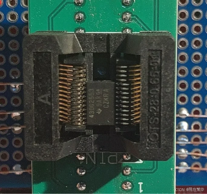
拔出芯片的时候最好是弄一个叫芯片起拔器的小夹子

注意,不是钩子的!!钩子款是拔四方芯片的,我一开始也买错成这种了。错的型号图片就不放上来了。
有两块五的型号
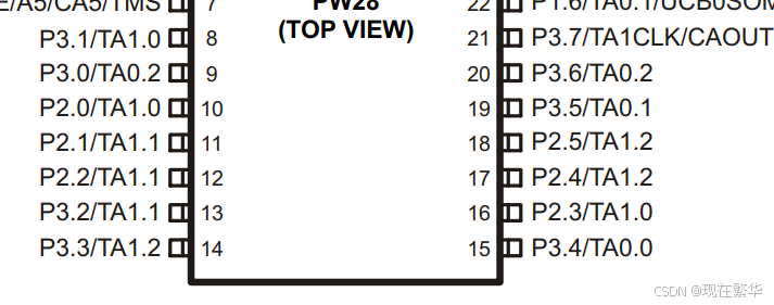
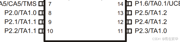
tssop-20和tssop-28的
28的多p3端口,但是从虚线往下的定义都不一样了,所以对20的版本不完全向下兼容
20的版本可以完全替代直插的型号
所以这样我买了一个tssop28转pdip的插座,注意,他是方针的,可插不进芯片的圆孔里
芯片的⚪点是一号腿
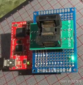
我把编程用的引脚,灯,按钮引出,额外对左下角的pin连接了一个led用以验证后边的步骤
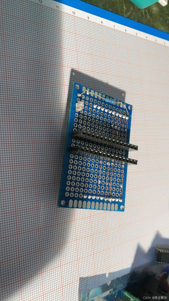
当然,安装这些附件前一定要把自带的芯片拆下!!!
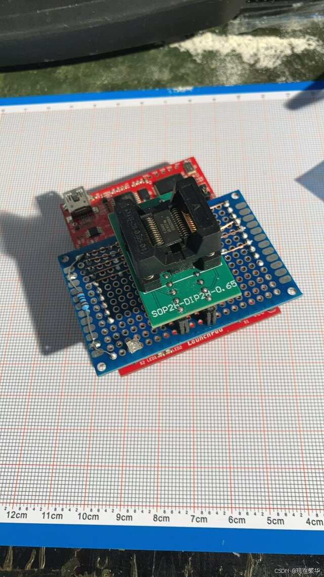
实物非常帅的。。只是摄像头不还原色彩。
那么原来的2553lp是不支持p3,所以要新作一个开发板(的顶)
我用一个小时的时间对着datasheet去重写了下边这个头文件
相比官方的2553lp的头文件,修改的地方有,pin的形象注释和位置,特殊功能引脚(其中ss和sck没有验证过,TWI0 也一样),定时器位置(用以支持analogwrite,定时器的定义没有仔细研究,所以都没有使用TAx.0,注意到所有使用同一个定时器编号的引脚是不可以同时输出pwm的),位操作位置,a6a7位置,
/*
  ************************************************************************
  *   pins_energia.h
  *
  *   Energia core files for MSP430 spcial version for 28 pin tssop
  *      Copyright (c) 2025 Fanhua-BI4NDS. All right reserved.
  *
  *     Contribution: BI4NDS
  *
  ***********************************************************************
  Derived from:
  pins_arduino.h - Pin definition functions for Arduino
  Part of Arduino - http://www.arduino.cc/

  Copyright (c) 2007 David A. Mellis && 2025 BI4NDS

  This library is free software; you can redistribute it and/or
  modify it under the terms of the GNU Lesser General Public
  License as published by the Free Software Foundation; either
  version 2.1 of the License, or (at your option) any later version.

  This library is distributed in the hope that it will be useful,
  but WITHOUT ANY WARRANTY; without even the implied warranty of
  MERCHANTABILITY or FITNESS FOR A PARTICULAR PURPOSE.  See the GNU
  Lesser General Public License for more details.

  You should have received a copy of the GNU Lesser General
  Public License along with this library; if not, write to the
  Free Software Foundation, Inc., 59 Temple Place, Suite 330,
  JInan, SD  250002 CN
*/

#ifndef Pins_Energia_h
#define Pins_Energia_h
#ifndef BV
#define BV(x) (1 << (x))
#endif

static const uint8_t SS      = 8;  /* P3.1 */
static const uint8_t SCK     = 7;  /* P1.5 */
static const uint8_t MOSI    = 21; /* P1.7 */
static const uint8_t MISO    = 22; /* P1.6 */
static const uint8_t TWISCL1  = 11;   /* P2.1 SW I2C */
static const uint8_t TWISDA1  = 12;  /* P2.2 SW I2C */
static const uint8_t TWISDA0  = 21;  /* P1.7 */
static const uint8_t TWISCL0  = 22;  /* P1.6 */

static const uint8_t DEBUG_UARTRXD = 4;  /* Receive  Data (RXD) at P1.2 */
static const uint8_t DEBUG_UARTTXD = 3;  /* Transmit Data (TXD) at P1.1 */
#define TWISDA1_SET_MODE  (INPUT)
#define TWISCL1_SET_MODE  (INPUT)
#if defined(__MSP430_HAS_USCI__)
#define TWISDA0_SET_MODE  (PORT_SELECTION0 | PORT_SELECTION1 /* | INPUT_PULLUP*/) /* do not enable the pull ups for this device */
#define TWISCL0_SET_MODE  (PORT_SELECTION0 | PORT_SELECTION1 /* | INPUT_PULLUP*/)
#define DEBUG_UARTRXD_SET_MODE (PORT_SELECTION0 | PORT_SELECTION1 | INPUT)
#define DEBUG_UARTTXD_SET_MODE (PORT_SELECTION0 | PORT_SELECTION1 | OUTPUT)
#define SPISCK_SET_MODE (PORT_SELECTION0 | PORT_SELECTION1)
#define SPIMOSI_SET_MODE (PORT_SELECTION0 | PORT_SELECTION1)
#define SPIMISO_SET_MODE (PORT_SELECTION0 | PORT_SELECTION1)
#endif
#if defined(__MSP430_HAS_USI__)
#define TWISDA0_SET_MODE  (PORT_SELECTION0 | INPUT_PULLUP)
#define TWISCL0_SET_MODE  (PORT_SELECTION0 | INPUT_PULLUP)
#define DEBUG_UARTRXD_SET_MODE (PORT_SELECTION0 | INPUT)
#define DEBUG_UARTTXD_SET_MODE (PORT_SELECTION0 | OUTPUT)
#define SPISCK_SET_MODE (PORT_SELECTION0)
#define SPIMOSI_SET_MODE (PORT_SELECTION0)
#define SPIMISO_SET_MODE (PORT_SELECTION0)
#endif

/* Define the default I2C settings */
#define DEFAULT_I2C -1 /* indicates SW I2C on pseudo module 1 */
#define TWISDA TWISDA1
#define TWISCL TWISCL1
#define TWISDA_SET_MODE  TWISDA1_SET_MODE
#define TWISCL_SET_MODE  TWISCL1_SET_MODE

#define DEBUG_UART_MODULE_OFFSET 0x0

#define DEBUG_UART_MODULE 0x0

#define MSP430_HAS_PORT3_R  //new line

static const uint8_t A0  = 2;
static const uint8_t A1  = 3;
static const uint8_t A2  = 4;
static const uint8_t A3  = 5;
static const uint8_t A4  = 6;
static const uint8_t A5  = 7;
static const uint8_t A6  = 22;
static const uint8_t A7  = 23;
static const uint8_t A10 = 128 + 10; // special. This is the internal temp sensor

//                      +-\/-+
//               VCC   1|    |28  GND
//         (A0)  P1.0  2|    |27  XIN   P2.6
//         (A1)  P1.1  3|    |26  XOUT  P2.7
//         (A2)  P1.2  4|    |25  TEST
//         (A3)  P1.3  5|    |24  RST#
//         (A4)  P1.4  6|    |23  P1.7  (A7) (SCL) (MISO) depends on chip
//         (A5)  P1.5  7|    |22  P1.6  (A6) (SDA) (MOSI)
//               ----------------------
//               P2.0  8|    |21  P2.5
//               P2.1  9|    |20  P2.4
//               P2.2 10|    |19  P2.3
//               P2.0 11|    |18  P2.5
//               P2.0 12|    |17  P2.5
//               P2.0 13|    |16  P2.5
//               P2.0 14|    |15  P2.5
//                      +----+
//

// Pin names based on the silkscreen
//
static const uint8_t P1_0 = 2;
static const uint8_t P1_1 = 3;
static const uint8_t P1_2 = 4;
static const uint8_t P1_3 = 5;
static const uint8_t P1_4 = 6;
static const uint8_t P1_5 = 7;
//-----------------------------
static const uint8_t P3_1 = 8;
static const uint8_t P3_0 = 9;

static const uint8_t P2_0 = 10;
static const uint8_t P2_1 = 11;
static const uint8_t P2_2 = 12;

static const uint8_t P3_2 = 13;
static const uint8_t P3_3 = 14;
static const uint8_t P3_4 = 15;

static const uint8_t P2_3 = 16;
static const uint8_t P2_4 = 17;
static const uint8_t P2_5 = 18;

static const uint8_t P3_5 = 19;
static const uint8_t P3_6 = 20;
static const uint8_t P3_7 = 21;

static const uint8_t P1_6 = 22;
static const uint8_t P1_7 = 23;

static const uint8_t P2_7 = 26;
static const uint8_t P2_6 = 27;

static const uint8_t RED_LED = 2;
static const uint8_t GREEN_LED = 22;
static const uint8_t PUSH2 = 5;

static const uint8_t TEMPSENSOR = 128 + 10; // depends on chip


#ifdef ARDUINO_MAIN

const uint16_t port_to_input[] = {
   NOT_A_PORT,
   (const uint16_t) (&P1IN),
   (const uint16_t) (&P2IN),
#ifdef __MSP430_HAS_PORT3_R__
   (const uint16_t) (&P3IN),
#endif
};

const uint16_t port_to_output[] = {
   NOT_A_PORT,
   (const uint16_t) (&P1OUT),
   (const uint16_t) (&P2OUT),
#ifdef __MSP430_HAS_PORT3_R__
   (const uint16_t) (&P3OUT),
#endif
};

const uint16_t port_to_dir[] = {
   NOT_A_PORT,
   (const uint16_t) (&P1DIR),
   (const uint16_t) (&P2DIR),
#ifdef __MSP430_HAS_PORT3_R__
   (const uint16_t) (&P3DIR),
#endif
};

const uint16_t port_to_ren[] = {
   NOT_A_PORT,
   (const uint16_t) (&P1REN),
   (const uint16_t) (&P2REN),
#ifdef __MSP430_HAS_PORT3_R__
   (const uint16_t) (&P3REN),
#endif
};

const uint16_t port_to_sel0[] = {  /* put this PxSEL register under the group of PxSEL0 */
   NOT_A_PORT,
   (const uint16_t) (&P1SEL),
   (const uint16_t) (&P2SEL),
#ifdef __MSP430_HAS_PORT3_R__
   (const uint16_t) (&P3SEL),
#endif
};

const uint16_t port_to_sel2[] = {
   NOT_A_PORT,
#if (defined(P1SEL2_) || defined(P1SEL2) || defined(__MSP430_HAS_P1SEL2__))
   (const uint16_t) (&P1SEL2),
#else
        NOT_A_PORT,
#endif
#if (defined(P2SEL2_) || defined(P2SEL2) || defined(__MSP430_HAS_P2SEL2__))
   (const uint16_t) (&P2SEL2),
#else
        NOT_A_PORT,
#endif
#if (defined(P3SEL2_) || defined(P3SEL2) || defined(__MSP430_HAS_P3SEL2__))
   (const uint16_t) (&P3SEL2),
#else
        NOT_A_PORT,
#endif
};


/*
 * Defines for devices with 2x TA3 timers (e.g. MSP430g2553). On the 20pin devices, upto 3 analog outputs are available
 * T0A1, T1A1 and T1A2
 */
const uint8_t digital_pin_to_timer[] = {
   NOT_ON_TIMER, /*  dummy */
   NOT_ON_TIMER, /*  1 - VCC */
   NOT_ON_TIMER, /*  2 - P1.0 */
   NOT_ON_TIMER, /*  3 - P1.1, note: A0 output cannot be used with analogWrite */
   T0A1,         /*  4 - P1.2 */
   NOT_ON_TIMER, /*  5 - P1.3 */
   NOT_ON_TIMER, /*  6 - P1.4 note: special case. Leaving as no timer due to difficulty determining if available */
   NOT_ON_TIMER, /*  7 - P1.5 note: A0 output cannot be used with analogWrite  */
//---------------------------------
   NOT_ON_TIMER,       /*  8 - P3.1 note: A0 output cannot be used with analogWrite */
   T0A2,
   NOT_ON_TIMER, /*  10 - P2.0 note: A0 output cannot be used with analogWrite */
   T1A1,
   T1A1,
   T1A1,
   T1A2,         /* 14 - P3.3 */
   NOT_ON_TIMER, /* 15 - P3.4 */
   NOT_ON_TIMER, /* 16 - P2.3 */
   T1A2,         /* 17 - P2.4 */
   T1A2,
   T0A1,         /* 19 - P3.5*/
   T0A2,
   NOT_ON_TIMER, /* 21 - P3.7 */
   T0A1,         /* 22 - P1.6 */
   NOT_ON_TIMER,
   NOT_ON_TIMER,
   NOT_ON_TIMER,
   NOT_ON_TIMER,
   NOT_ON_TIMER,
   T0A1,         /* 27 - XIN - P2.6: */
   NOT_ON_TIMER, /* 28 - GND */
};

const uint8_t digital_pin_to_port[] = {
   NOT_A_PIN, /* dummy */
   NOT_A_PIN, /* 1 */
   P1, /* 2 */
   P1, /* 3 */
   P1, /* 4 */
   P1, /* 5 */
   P1, /* 6 */
   P1, /* 7 */
   //------------
   P3, /* 8 */
   P3, /* 9 */

   P2, /* 10 */
   P2, /* 11 */
   P2, /* 12 */

   P3, /* 13 */
   P3, /* 14 */
   P3, /* 15 */

   P2, /* 16 */
   P2, /* 17 */
   P2, /* 18 */

   P3, /* 19 */
   P3, /* 20 */
   P3, /* 21 */

   P1, /* 22 */
   P1, /* 23 */

   NOT_A_PIN, /* 24*/
   NOT_A_PIN, /* 25 */
   P2, /* 26 */
   P2, /* 27 */
   NOT_A_PIN, /* 28 */
};

const uint8_t digital_pin_to_bit_mask[] = {
   NOT_A_PIN, /* 0,  pin count starts at 1 */
   NOT_A_PIN, /* 1,  VCC */
   BV(0),     /* 2,  port P1.0 */
   BV(1),     /* 3,  port P1.1 */
   BV(2),     /* 4,  port P1.2 */
   BV(3),     /* 5,  port P1.3*/
   BV(4),     /* 6,  port P1.4 */
   BV(5),     /* 7,  port P1.5 */
   //---------------------------
   BV(1),     /* 8,  port P3.1 */
   BV(0),     /* 9,  port P3.0 */

   BV(0),     /* 10, port P2.0 */
   BV(1),     /* 11, port P2.1 */
   BV(2),     /* 12, port P2.2 */

   BV(2),     /* 13, port P3.2 */
   BV(3),     /* 14, port P3.3 */
   BV(4),     /* 15, port P3.4 */

   BV(3),     /* 16, port P2.3 */
   BV(4),     /* 17, port P2.4 */
   BV(5),     /* 18, port P2.5 */

   BV(5),     /* 19, port P3.5 */
   BV(6),     /* 20, port P3.6 */
   BV(7),     /* 21, port P3.7 */

   BV(6),     /* 22, port P1.6 */
   BV(7),     /* 23, port P1.7 */


   NOT_A_PIN, /* 24, RST */
   NOT_A_PIN, /* 25, TEST */
   BV(7),     /* 26, XOUT */
   BV(6),     /* 27, XIN */
   NOT_A_PIN, /* 28, GND */
};
const uint32_t digital_pin_to_analog_in[] = {
        NOT_ON_ADC,     /*  dummy   */
        NOT_ON_ADC,     /*  1 - 3.3V*/
        0,            /*  2 - A0 */
        1,              /*  3 - A1 */
        2,             /*  4 - A2 */
        3,             /*  5 - A3 */
        4,             /*  6 - A4 */
        5,            /*  7 - A5 */
		//----------------------------
        NOT_ON_ADC,
		NOT_ON_ADC,
		NOT_ON_ADC,
		NOT_ON_ADC,
		NOT_ON_ADC,
		NOT_ON_ADC,
		NOT_ON_ADC,
		NOT_ON_ADC,
		NOT_ON_ADC,
		NOT_ON_ADC,
		NOT_ON_ADC,
		NOT_ON_ADC,
		NOT_ON_ADC,
		NOT_ON_ADC,
        6,              /*  22 - A6 */
        7,              /*  23 - A7 */
        NOT_ON_ADC,    /*   RST */
        NOT_ON_ADC,     /*  PF0 */
        NOT_ON_ADC,    /*   PE0 */
        NOT_ON_ADC,     /*   PB2 */
        NOT_ON_ADC     /*  28- GND */
};

#endif
#endif
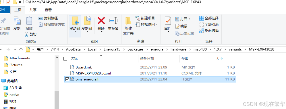
一定要注意,是放到energia15里,而不是exe的文件夹,其他文件用的是5529lp的文件,改了名称
#MSP-EXP43028

MSP-EXP43028.vid.0=0x2341
MSP-EXP43028.pid.0=0x0c9f

MSP-EXP43028.name=MSP-EXP430G2553-tssop28

MSP-EXP43028.build.mcu=msp430g2553
MSP-EXP43028.build.f_cpu=16000000L
MSP-EXP43028.build.core=msp430
MSP-EXP43028.build.variant=MSP-EXP43028
MSP-EXP43028.build.board=MSP-EXP43028
MSP-EXP43028.build.extra_flags=

MSP-EXP43028.upload.tool=mspdebug
MSP-EXP43028.upload.protocol=rf2500
MSP-EXP43028.upload.maximum_size=16384
MSP-EXP43028.upload.maximum_data_size=512
这个是在board。txt里加入的描述
一旦完成这些步骤,就应该有一个开发板
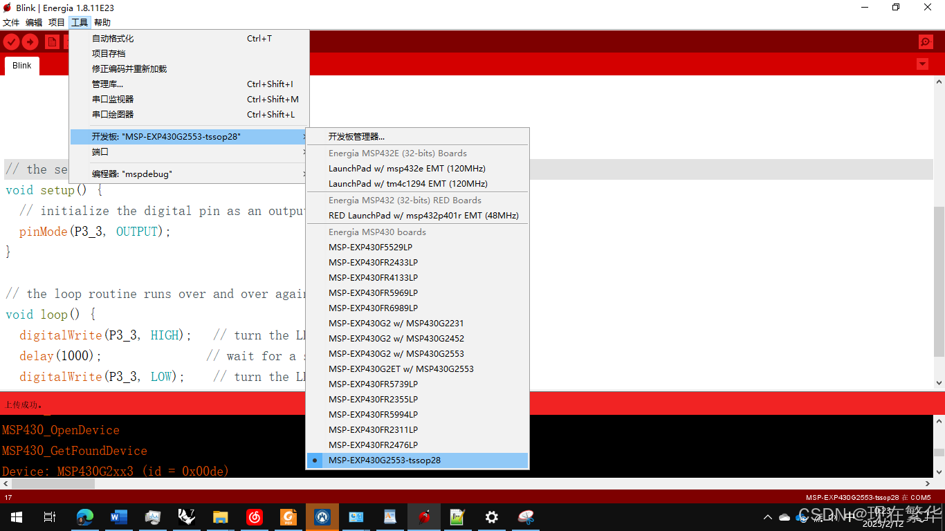
当然,开发板不要更新,要不然就没了
/*
  Blink
  The basic Energia example.
  Turns on an LED on for one second, then off for one second, repeatedly.
  Change the LED define to blink other LEDs.

  Hardware Required:
  * LaunchPad with an LED

  This example code is in the public domain.
*/


// the setup routine runs once when you press reset:
void setup() {
  // initialize the digital pin as an output.
  pinMode(P3_3, OUTPUT);
}

// the loop routine runs over and over again forever:
void loop() {
  digitalWrite(P3_3, HIGH);   // turn the LED on (HIGH is the voltage level)
  delay(1000);               // wait for a second
  digitalWrite(P3_3, LOW);    // turn the LED off by making the voltage LOW
  delay(1000);               // wait for a second
}
用这段程序验证
led可以闪烁
难点在于:
找到开发板包的位置,这比改官方头文件还难以下手
energia的硬件驱动需要单独安装,不是拷贝就能用的
吃顿健康营养的饭


 1272
1272

 被折叠的 条评论
为什么被折叠?
被折叠的 条评论
为什么被折叠?
 到【灌水乐园】发言


